Encore
Encore was an american company founded in 1983 by three famous computer industry minds: Gordon Bell, who was an engineering vice president of Digital Equipment Corp. (DEC), Kenneth G. Fisher, former CEO of Prime Computer and Henry Burkhardt III, co-founder of Data General. The newspaper computerworld wrote once that "the hopes and hype were at a feverish level." .
Obviously everybody expected a revolution in computer architecture. And their idea was revolutionary in the sense that they used a number of cheap commodity microprocessors to build a powerful multiprocessor system instead of building expensive single processor systems like the VAX from DEC or IBM with their System/370.
Multimax
Encore named their parallel processor system Multimax. The central piece was a high speed bus called Nanobus. This bus had 32 address bits and 64 data bits. It could transfer one word every 80 nanoseconds. The bandwith was 100 Mbytes/second which was a lot in the middle of the 1980's. Four different cards could be attached to the bus: a "Dual Processor Card" (DPC) with two CPUs and cache memory, a "Shared Memory Card" (SMC) based on DRAM, a "Ethernet/Mass Storage Card" (EMC) and a "System Control Card" (SCC). The SMC was split into two banks and used ECC. The EMC had an own processer.
The backplane was called the Nanobus since the 20-slot version was about 1 foot long, which is the distance an electrical signal will travel in a nanosecond.
There were two different versions of the Multimax: one big system with 20 slots, called the -20, and a smaller one with 11 slots, called the -10. The "-" means the different generations. (The small system had 11 slots. Therefore the natural name would be -11 but I believe that the marketing department or who else choosed the -10 for a cleaner roadmap.) See Figure 1 and 2 for the system appearence.
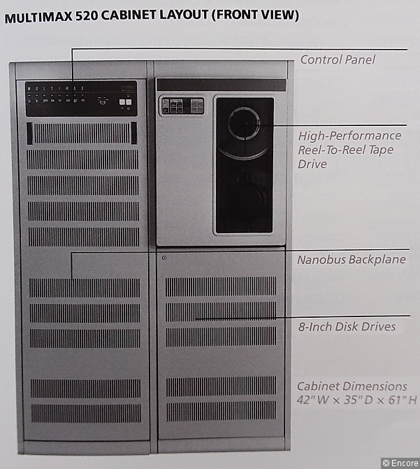
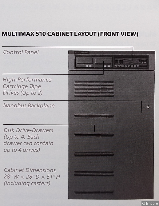
Fig. 1/2. The big Multimax shown on the left and the small Multimax shown one on the right.
Both systems were very flexible in their configuration. The big system could handle up to 10 processor cards with 20 CPUs. See Figure 3 for a summary of the different configurations.
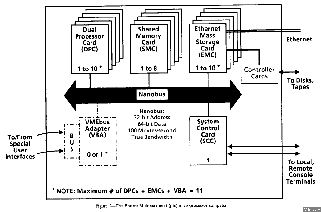
Fig. 3. The customer has many choices to configure his system.
The first system was the Multimax 120. This system used the NS32032 CPU. All multiprocessor systems based on this CPU faced the same problem: the CPU has only 24 address lines. National Semiconductor didn't expect a business in shared memory computers addressing more than 16 Mbytes. To overcome this problem engineers from Encore build a special hardware to expand the address bus from 24 bits to 32 bits.
The Multimax 120 was only sold in very little numbers, probably only once. Soon after the NS32032 Encore could use the NS32332 CPU and redesigned the DPC for them. They were called now "Advanced Dual Processor Card" (APC), see Figure 46. The rest of the system could be reused. The machines with the NS32332 were called Multimax 310 and Multimax 320.
The top-of-the-line systems were the Multimax 510 and Multimax 520 based on the NS32532 CPU. Again the CPU card was redesigned and became the "Extended Performance Dual Processor Card" (XPC). Two versions of this card were available: the XPC-01 used the 25 MHz CPU and the XPC-03 used the 30 MHz CPU. Encore claimed a performance of 8.5 MIPS for one NS32532 running at 30 MHz. A fully populated Multimax 520 was able to deliver 170 MIPS. Not bad for the 1980's!
Much more details about the hardware can be found in the 2nd chapter of the Multimax Technical Summary. Pete made it available and it can be downloaded here.
But Encore did not stop with the system approach at the Multimax level. They had a vision for the general concepts of providing compute power to large organizations. Figure 4 shows the general view.
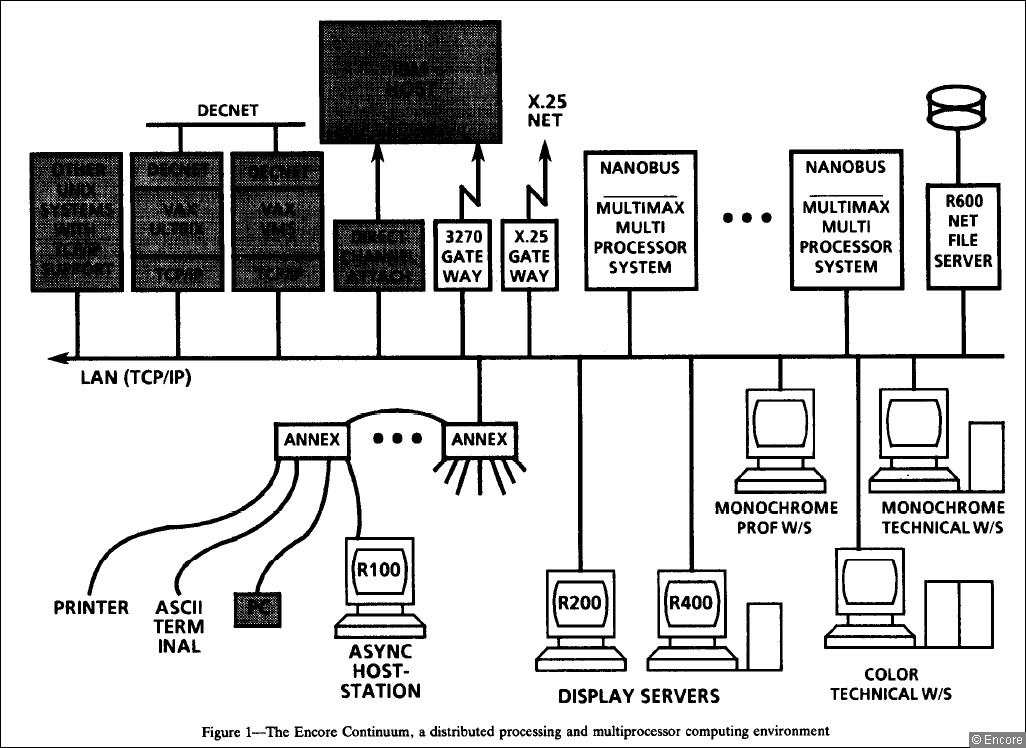
Fig. 4. How to do computing in the future in big organizations - the Encore view.
Encore reported an installed base of 101 Multimax systems as of Dec. 1, 1987 . This was not a big business for National Semiconductor even if every system contained 20 CPUs and all the other chips of Series 32000...
I got a nice photo from Pete showing a bottle of champagne which was given to every worker of Encore after they sold their first sytem:
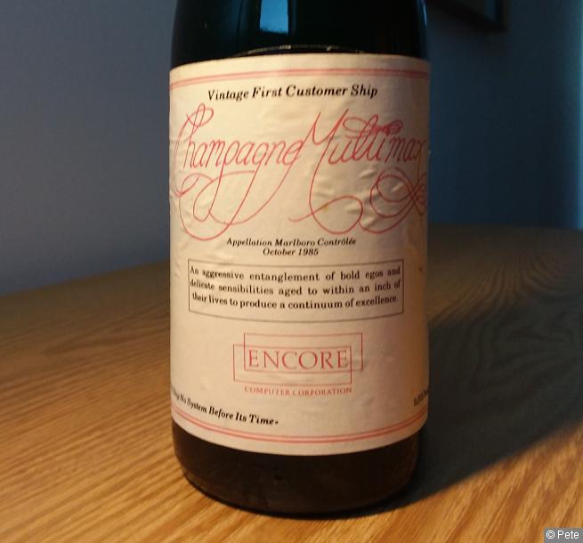
Fig. 5. Champagne is a good choice for a memorable moment.
Multimax at the Newcastle University, UK
The Newcastle University had two Multimax. The website about the 40th anniversary (1997) of the computer department write about them:
"The first SMP obtained for the parallelism work at Newcastle was an Encore Multimax 120. This system was purchased in July 1987 ... . This system (named "Turing") comprised 8 National Semiconductor 32032 CPUs running at 10 MHz (0.75 MIPS), with 16MB of main memory. This was a powerful system in those days, and provided a Unix service to the Department as well as supporting the parallelism work.
In 1988 Turing was upgraded to a Multimax 320, containing the next generation of CPU cards, that is to 8 National Semiconductor 32332 CPUs (15MHz, 2 MIPS), and provided faithful service including a long period without maintenance support, until it was decommissioned in 1996.
In 1988 a second Multimax (named "Newton") was acquired for the Centre for Multiprocessing. With additional upgrades from other projects, this machine, the first Multimax 520 in the country, comprised 14 National Semiconductor 32532 (30 MHz, 8.5 MIPS) and 128MB of main memory. Like Turing, Newton provided long and reliable service both to researchers as well as to Unix users in the Department. It is still running in 1997."
After Newton was switched off, it went to Jim Austin's computer museum - see below. Turing was scrapped ... maybe someone has a CPU board hanging on the wall.
The term SMP has somehow different meanings: some say shared-memory multiprocessor, other say symmetric multiprocessing.
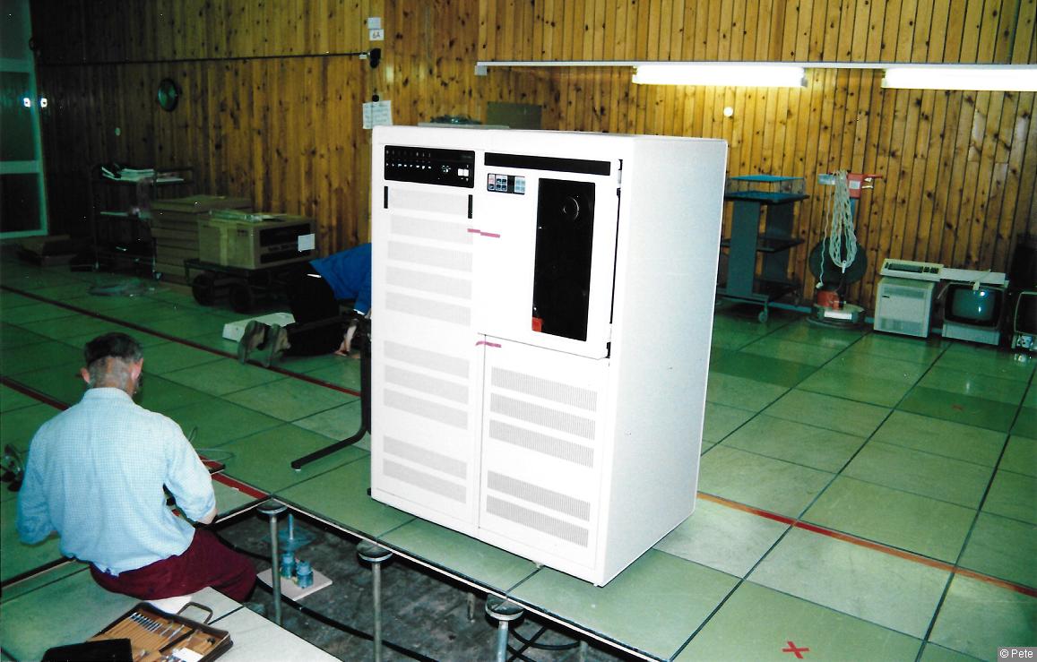
Fig. 6. The Multimax 120 during the installation procedure at Newcastle University in 1987.
The Multimax 520 at Jim Austin's Computer Museum
I was always curious to see a Multimax. For some years I knew only the system (link) located at the Computer History Museum in Moutain View, CA. In 2017 I learned that Jim Austin's computer museum in England owns a machine. In August 2018 the curiosity grew up and I asked Ed, who lives in England, whether he wants to visit the museum too. He said "yes" and we both were on the way on the 15 September 2018. It was a rainy day - perfect weather for a visit of a museum.
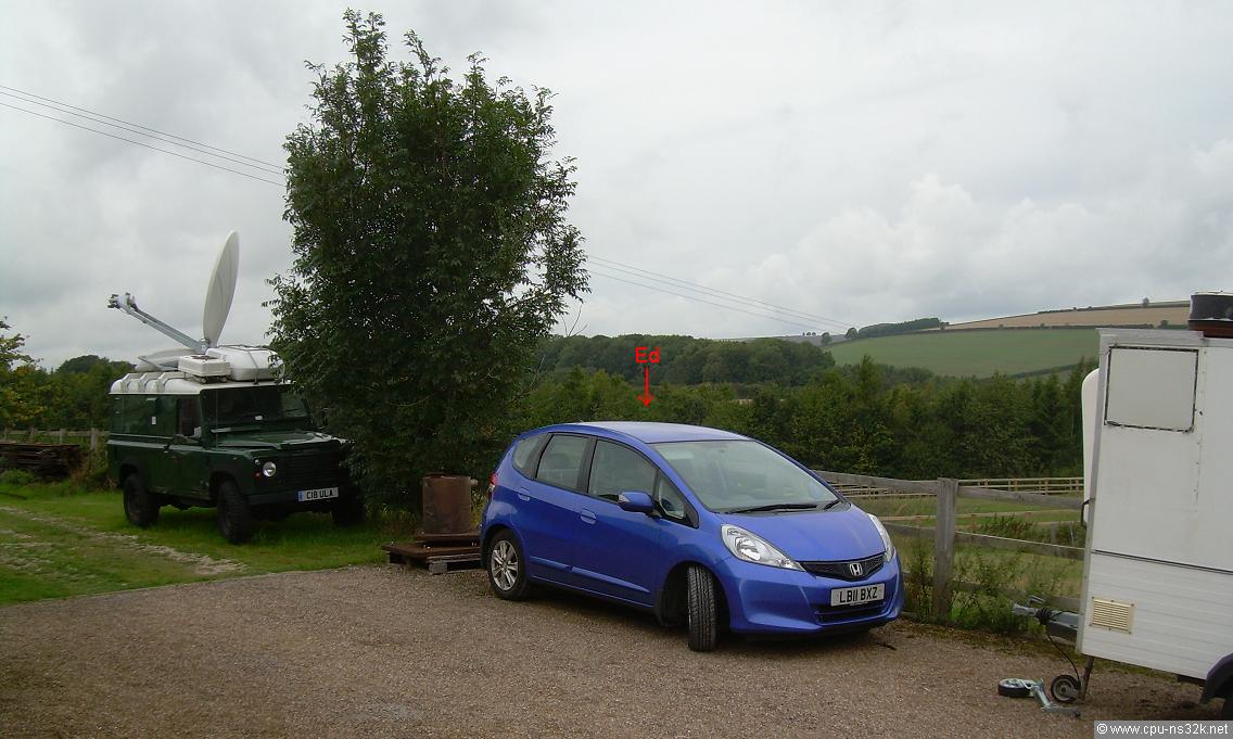
Fig. 7. Ed and I in the middle of nowhere: "Has anybody seen a Multimax?"
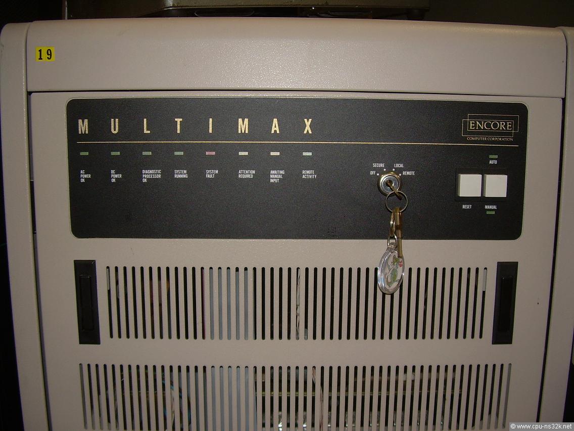
Fig. 8. "I am here.". Now the search is over.
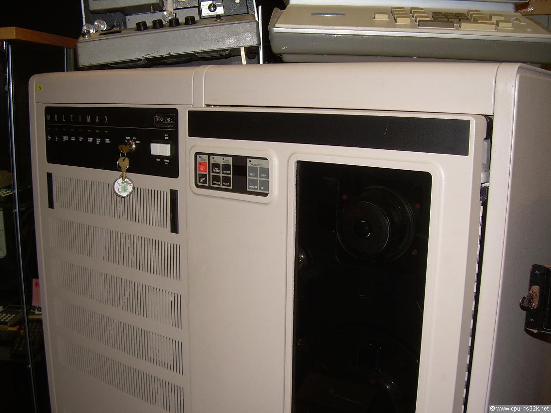
Fig. 9. There was no space to take a better photo of the frontside.
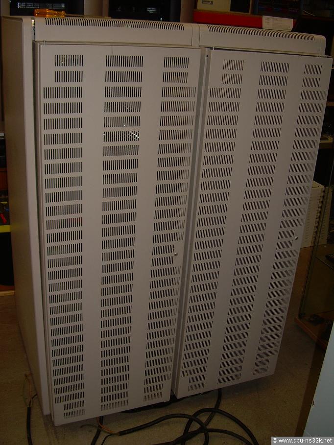
Fig. 10. But there was enough space to take a photo of the complete backside. Somehow boring view...
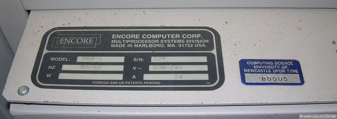
Fig. 11. It is interesting to note that there is no label saying: "I'm a Multimax 520".
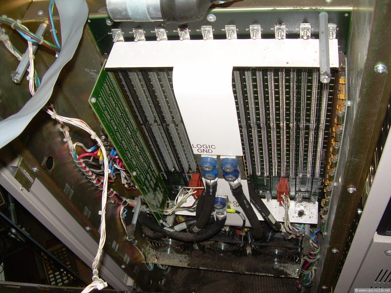
Fig. 12. A first look in the inside from the frontside: wow! Fat cables telling that there is a lot of power consumed.
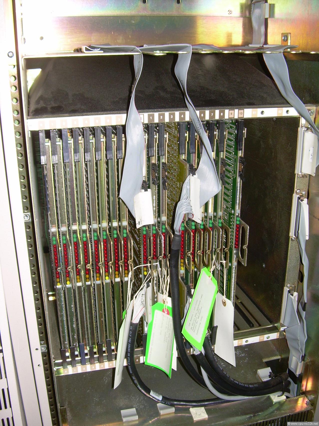
Fig. 13. And here are the user of all the power. A look from the backside showing all the boards that make this machine so powerful.
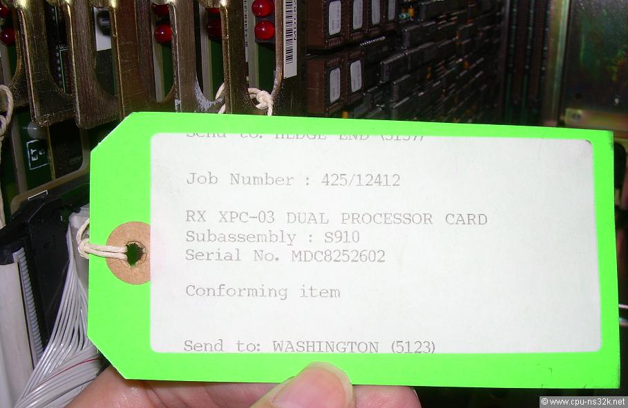
Fig. 14. The XPC-03 on the label tells the customer that this CPU board is using the 30 MHz NS32532 CPU.
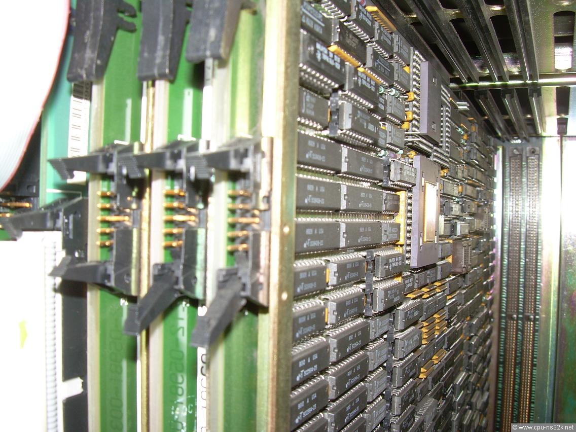
Fig. 15. Diving into the depth of the machine... in the backgroud on the right the backplane is visible with two additional sockets for more cards.
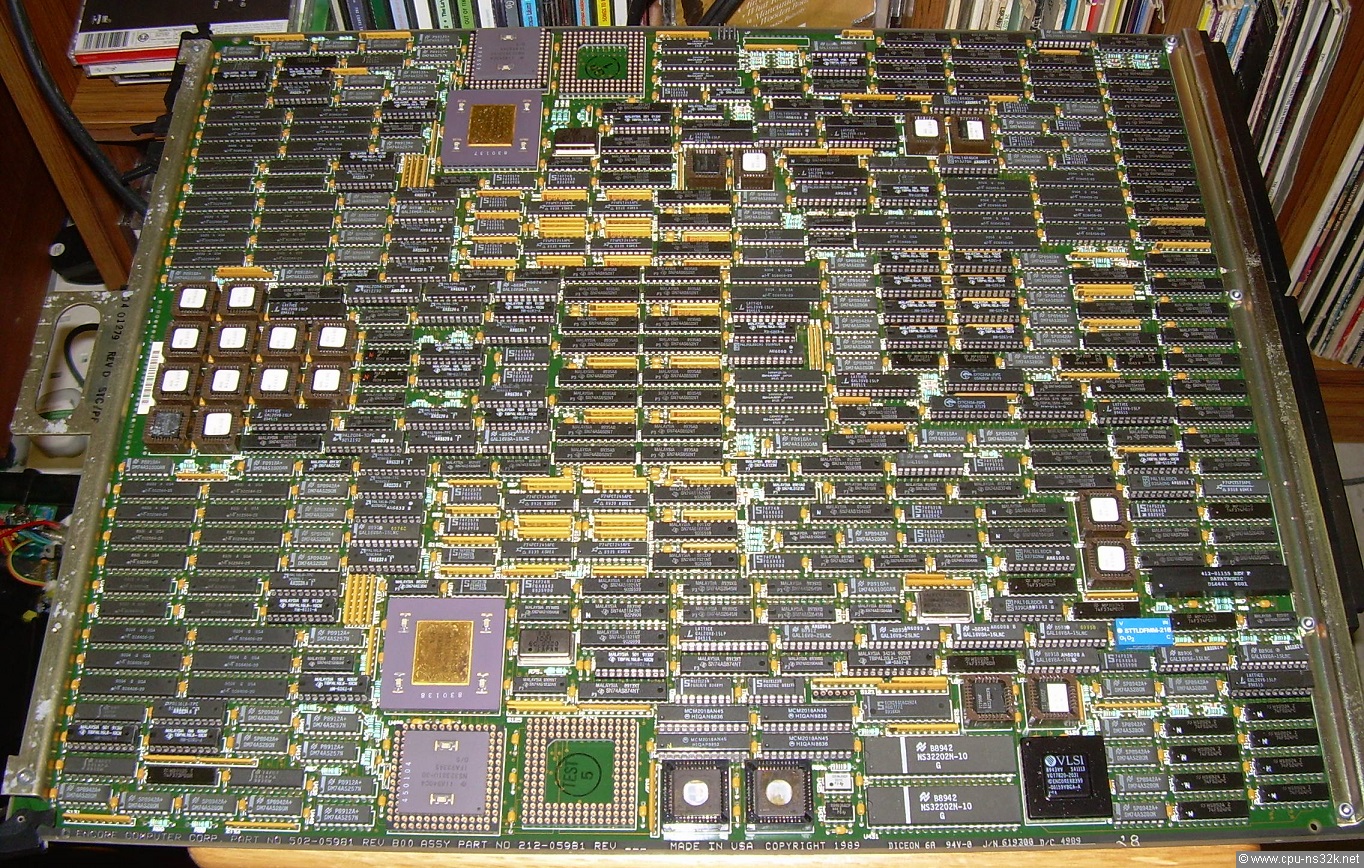
Fig. 16. This is one of the CPU boards - I never saw a Series 32000 based board of this size!!! Jim's machine has six of them.
I have never designed a board of this size. I wonder how Encore made the decision for the size: did they have a complete design in the beginning and fit the board size for the first machine to all the chips needed? Or was the board size fixed and the designer had to take some chips out? This maybe the case for the later CPU boards when the size was alredy fixed.
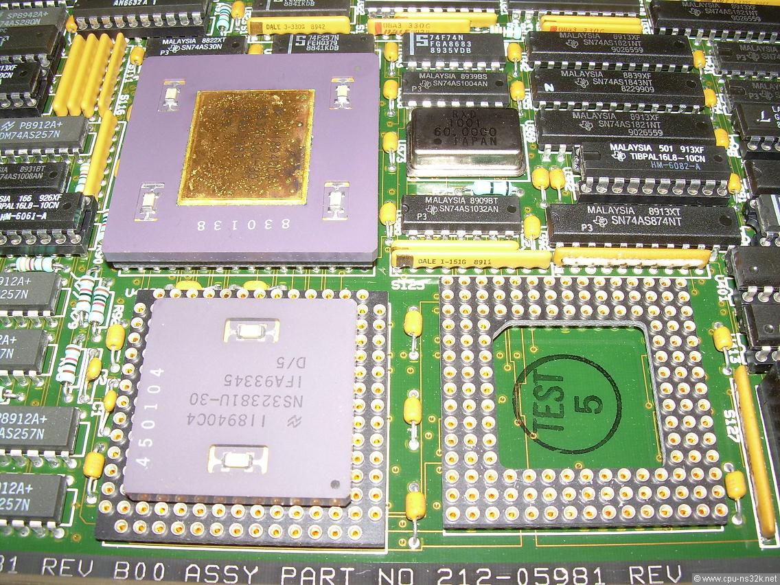
Fig. 17. A closer look to one of the CPU groups. For years I was looking for 30 MHz parts - here they are!
Please note that each CPU group has its own 60 MHz oscillator. Therefore all CPUs in the system are running asynchronously. But at the end they must be synchronized to the Nanobus. This requires a lot of logic - a good reason for the size of the boards.
The empty socket is for the Weitek floating-point processor. Obviously the CPU board is designed to be upgraded later when the interface chip NS32580 became available. Whether this upgrade had ever been happen to another Multimax would be interesting to know.
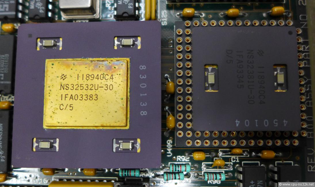
Fig. 18. All the NS32532 CPUs Ed and I have seen are looking like the one shown in this Figure. I'm no expert, but it doesn't look healthy!
In my opinion the CPUs were getting simply to hot. Although there is big fan at the top, the space between the CPU boards is very narrow. I doubt that the air stream was sufficient for cooling the CPUs. As a board designer I would have put a heatsink on them to avoid any later issues. Of course, it is not simple to fix a heatsink hanging in a strong air stream...
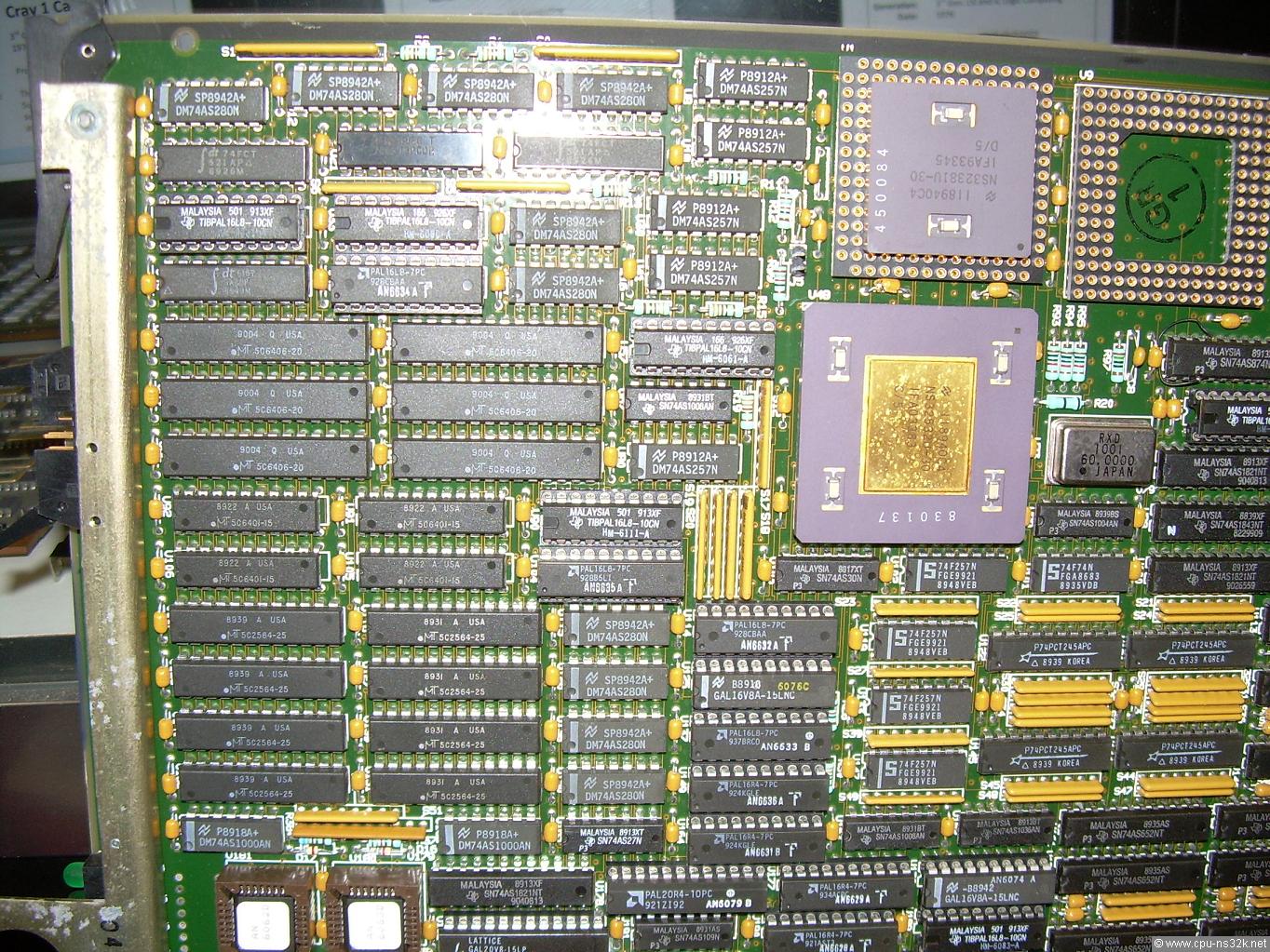
Fig. 19. The top CPU group and its cache made of three different SRAM chips from Micron.
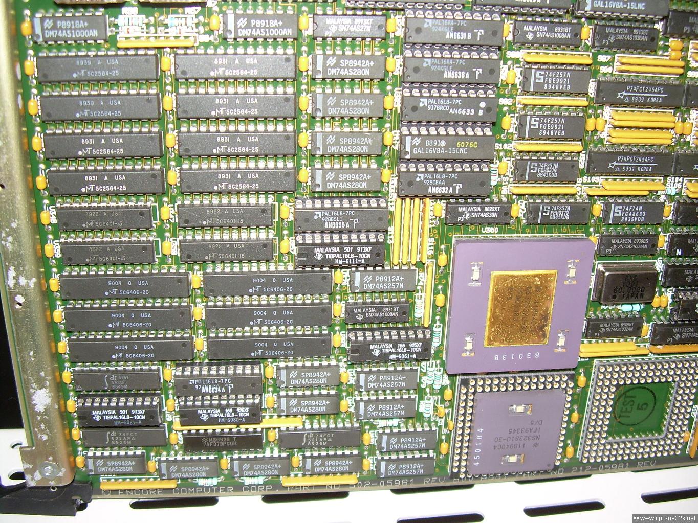
Fig. 20. The bottom CPU group is build identical to the top one.
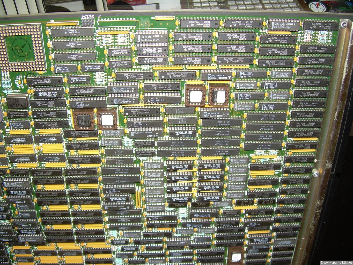
Fig. 21. The logic near the connector must be the Nanobus interface. It uses a lot of SRAM chips for unknown purposes.
Although it looks like I have bent the boards in the last figures, it is a "feature" of my old camera when taking photos in a small distance.
Fig. 22. The backside of the CPU board presented by Ed shows no wire. It would be interesting to know how many iterations were necessary to achieve this result.
Fig. 23. The next board we wanted to see was the memory board. Jim's machine has 8 of it each having 16 MB of DRAM for a total of 128 MB .
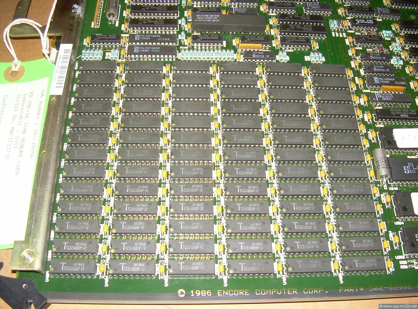
Fig. 24. One half of the DRAM array showing 6 columns by 13 rows of 1 Mbit memory chips from Toshiba.
The sum of the chips is 78 which is a very unusual number - I have never seen a similar configuration. Any explanation is welcome.
Summer 2019: Ed found the right answer. The next image shows the SN74ALS632 error detection and correcting device (EDAC). This device adds 7 check bits to 32 bits of data: 32 + 7 = 39. Two banks need 2 * 39 = 78 memory chips because the data port of each DRAM (TC511000 of Toshiba) is only one bit wide. Todays systems use 64 data bits and 8 check bits which is more efficient.
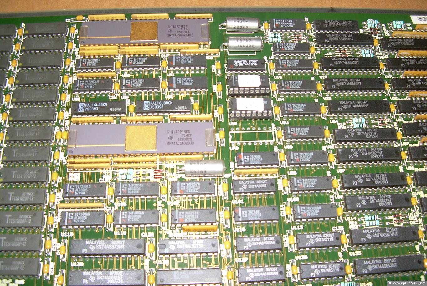
Fig. 25. The SN74ALS632 from Texas Instruments is an error detection and correcting device.
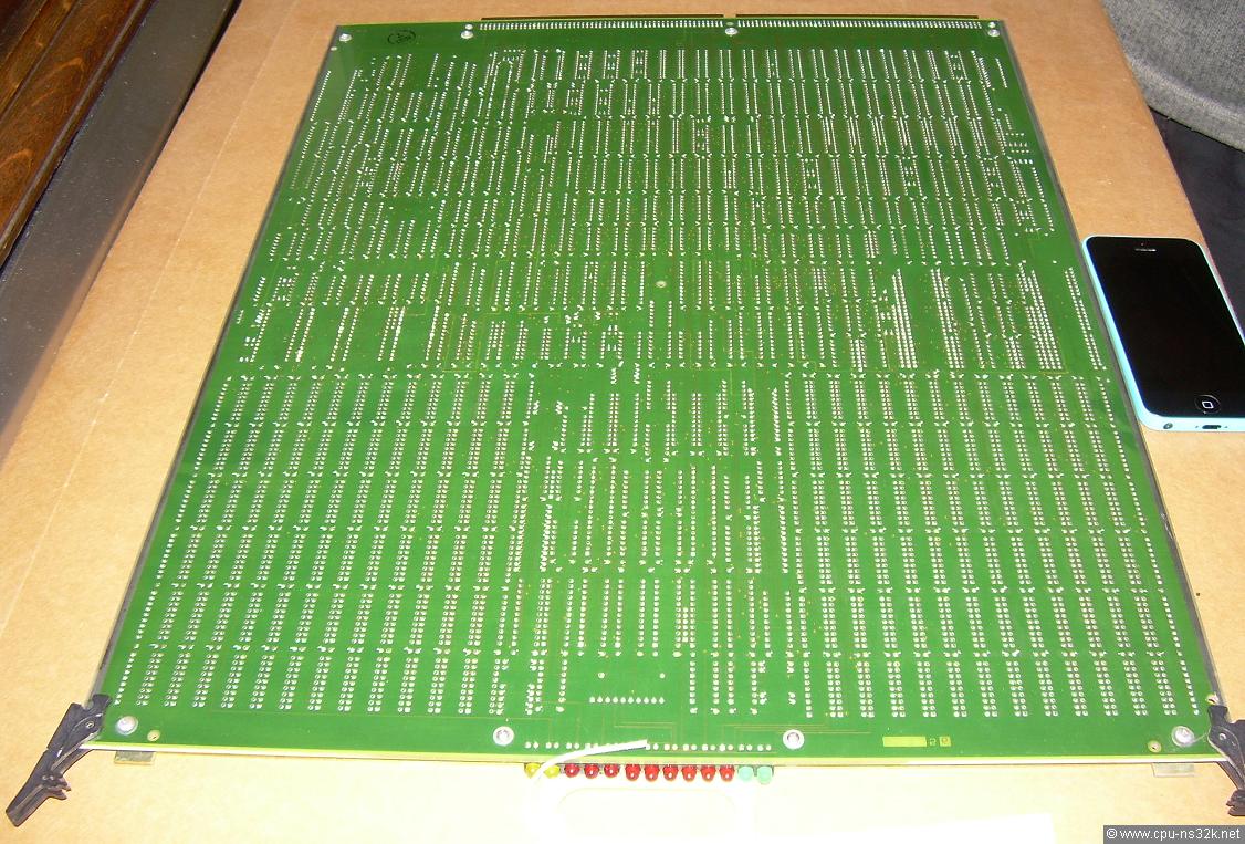
Fig. 26. The backside of the memory board is perfect like the CPU board.

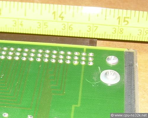
Fig. 27/28. It was time to measure the size of the giant boards: 49 cm * 38,8 cm, in other words 19,3 inch * 15,3 inch.
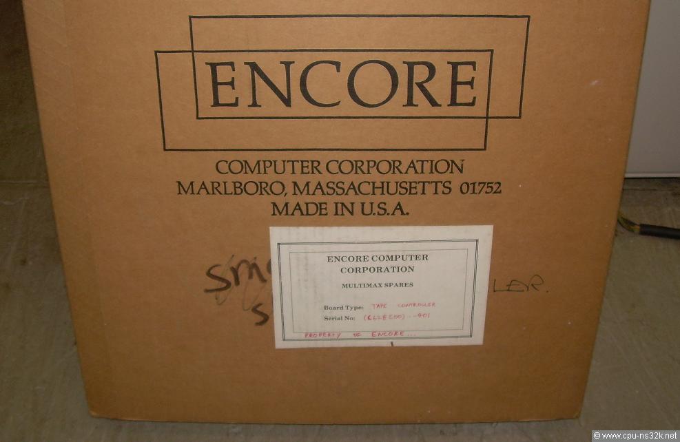
Fig. 29. Jim got also the spare parts in original package.
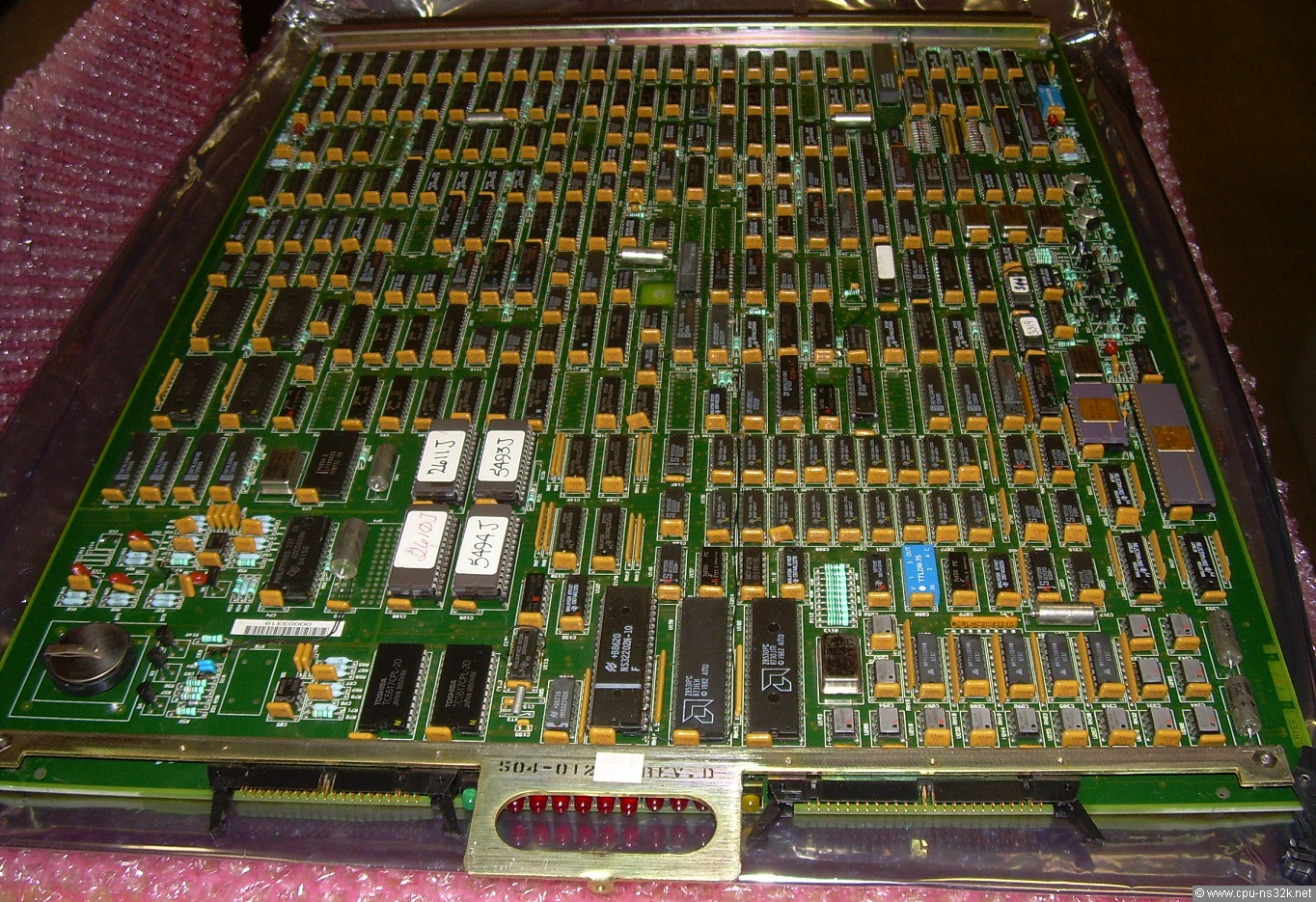
Fig. 30. The package says that this a tape controller.
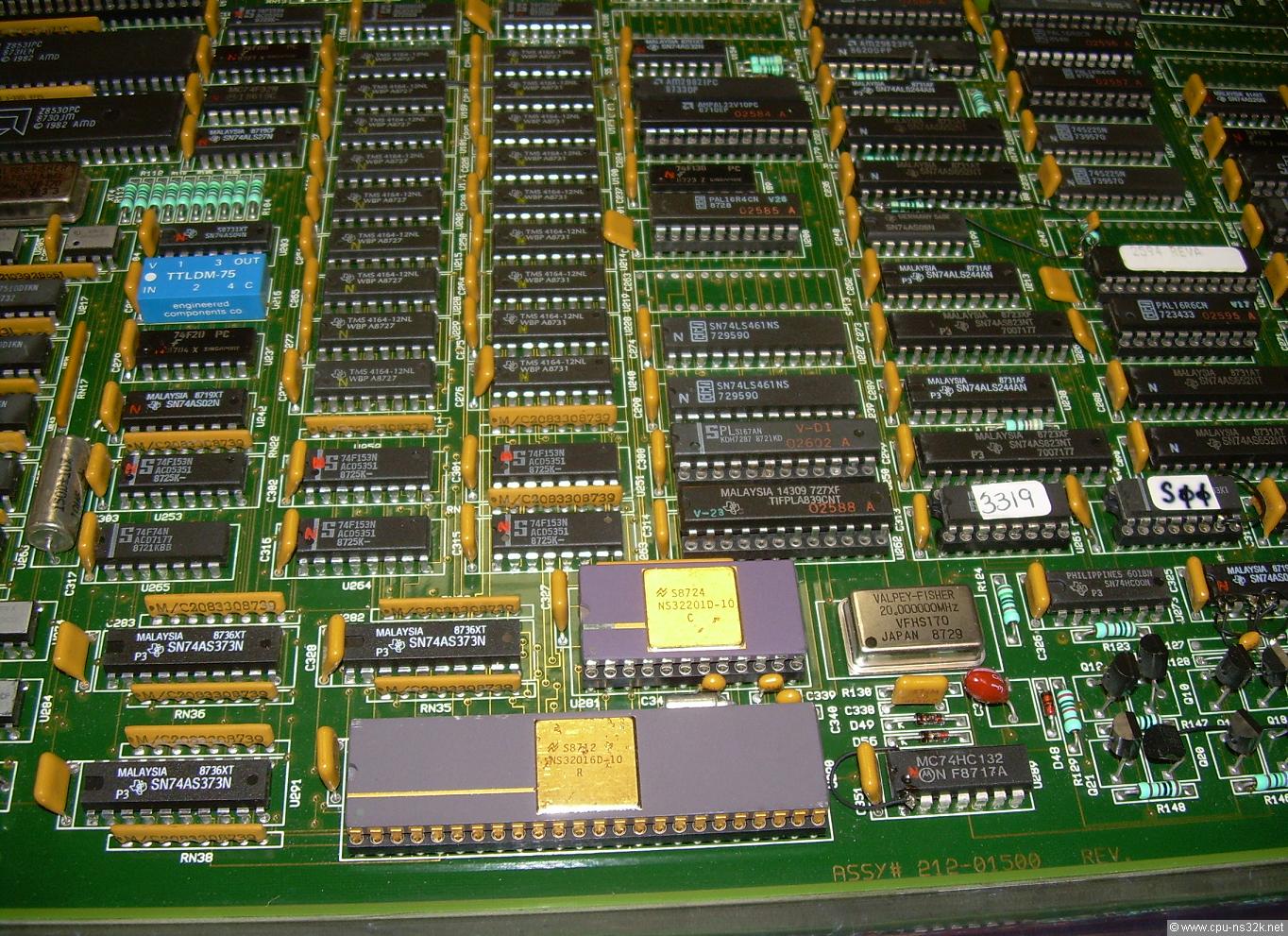
Fig. 31. The tape controller uses a NS32016 CPU as the main processor.
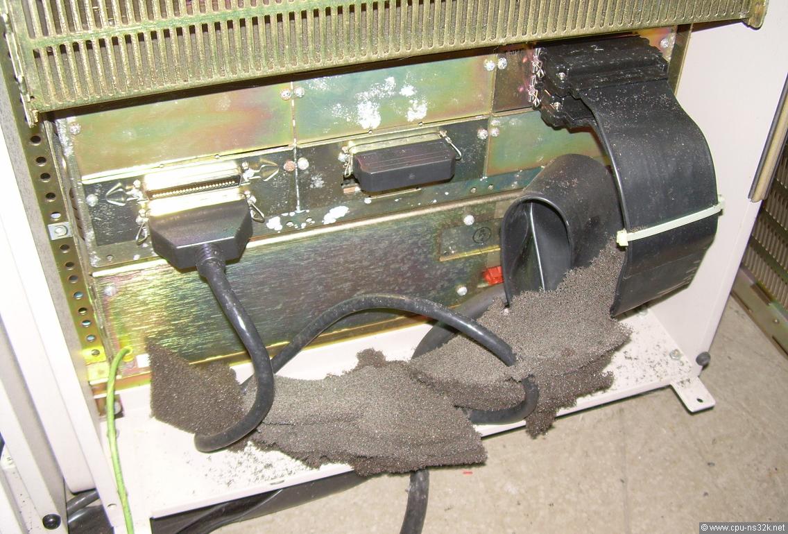
Fig. 32. The machine is old - no doubt!

Fig. 33. Coming back to the frontside showing the impressive backplane.
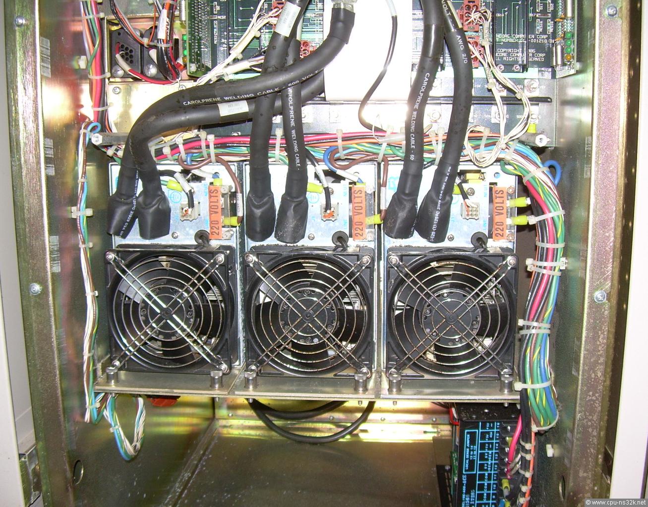
Fig. 34. Three power supplies are needed or they are used in a redundant configuration.
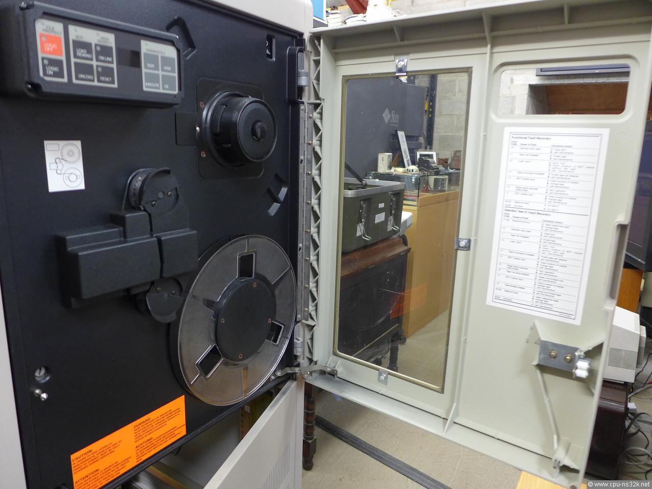
Fig. 35. The tape unit is in my view a monster from ancient times.
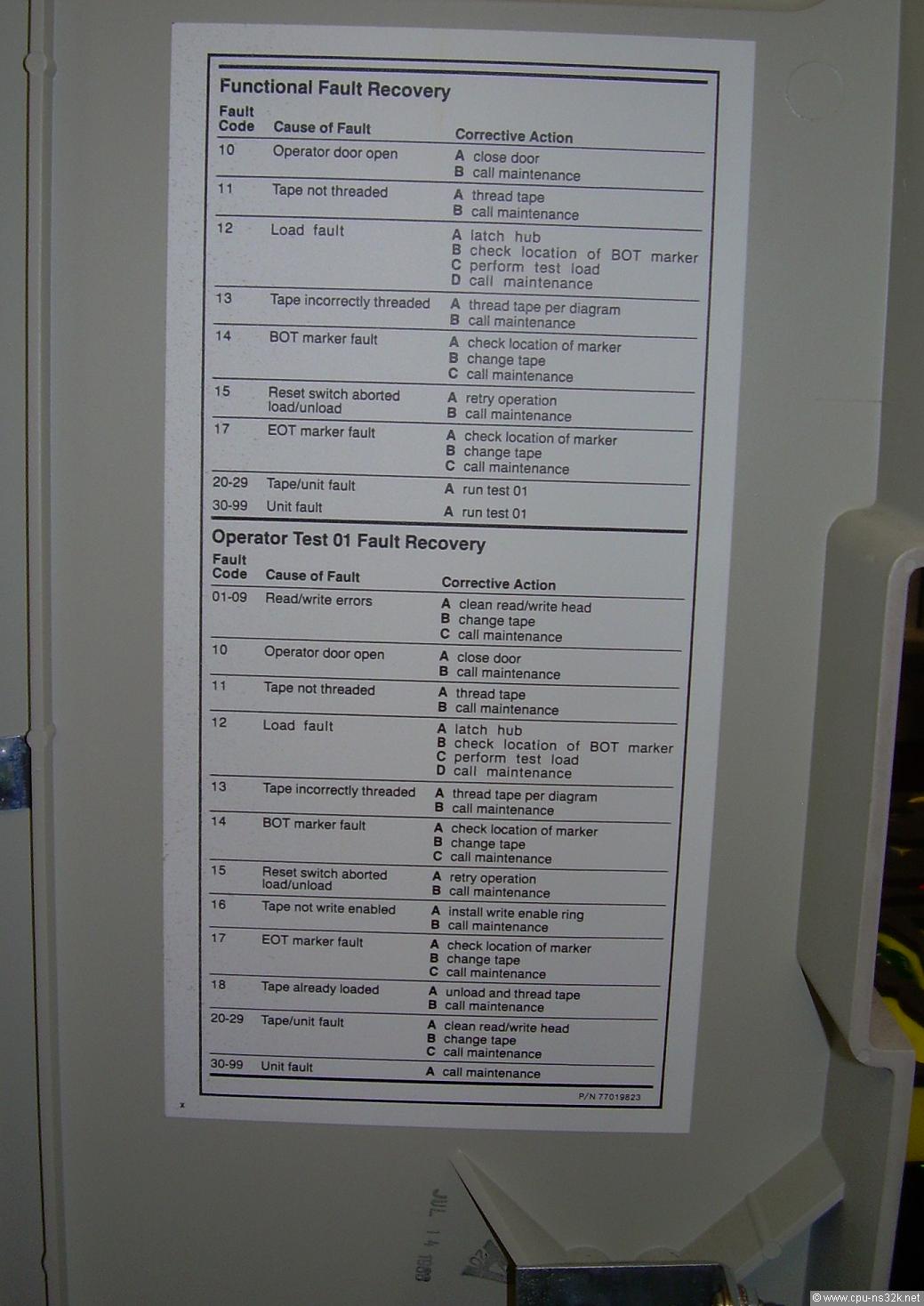
Fig. 36. The instruction list says always final call maintance if anything goes wrong with a tape or the tape unit.
Please note the date at the bottom: Jul 14 1988 . Maybe this was the final test date.
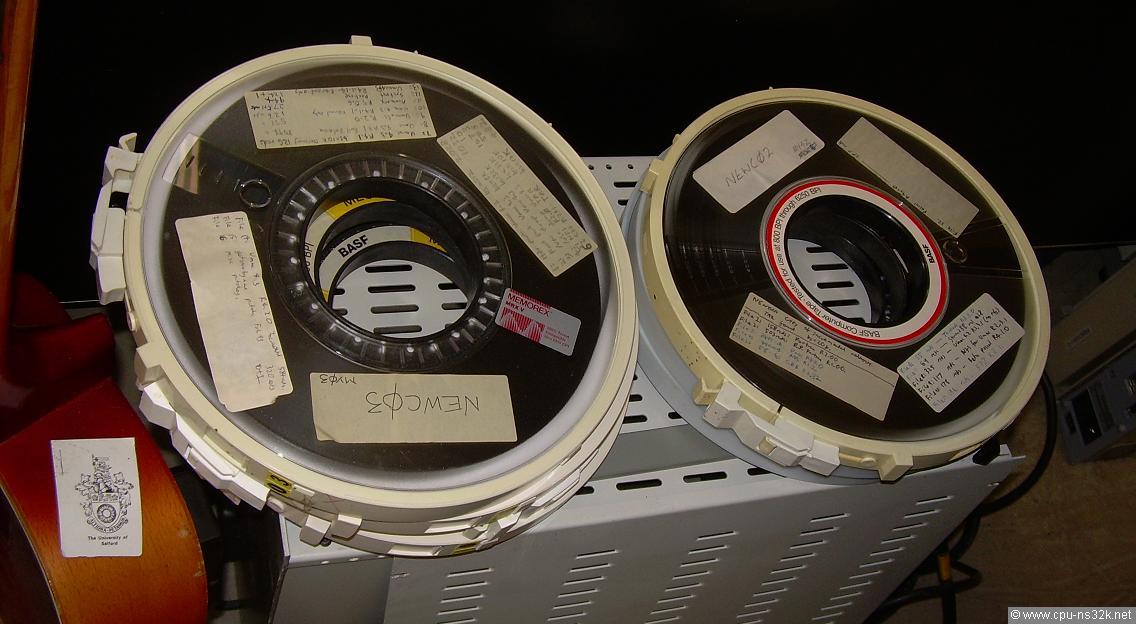
Fig. 37. Jim got also some tapes for the machine.
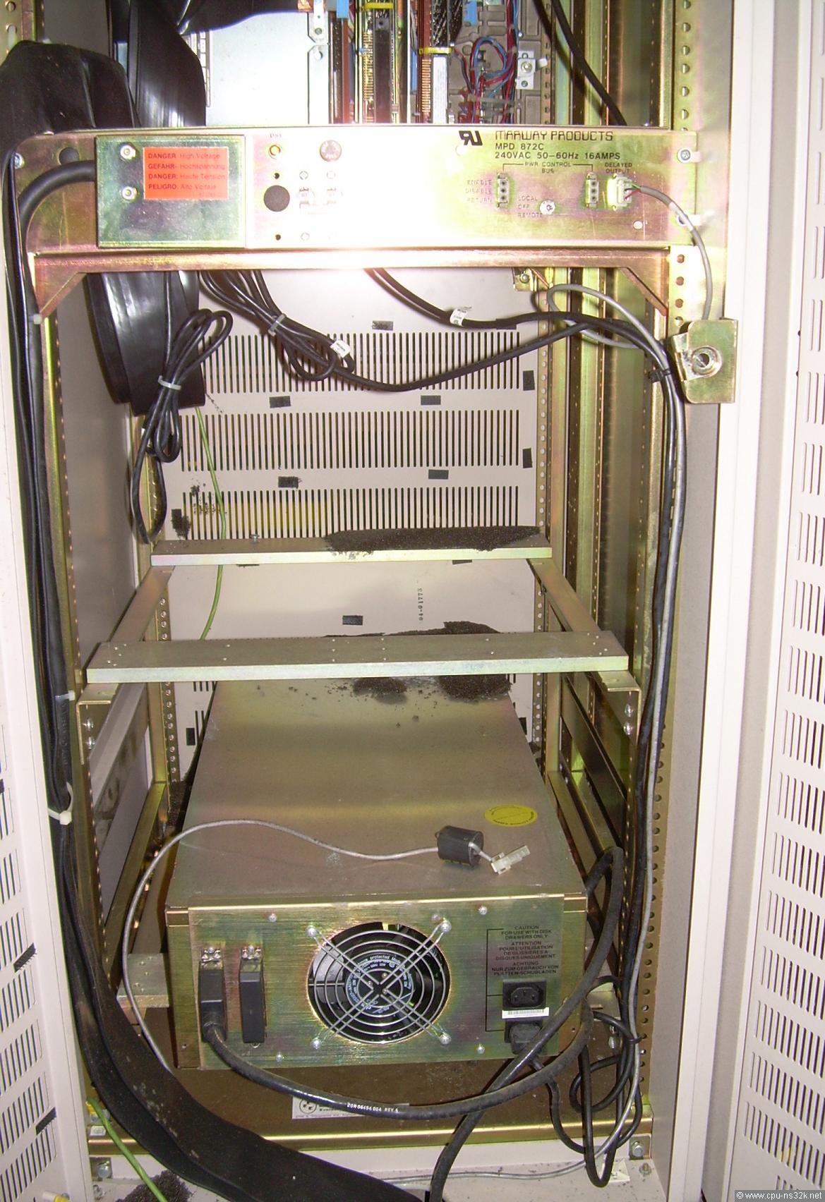
Fig. 38. The peripheral half of the system is relativly empty. At the bottom there are the hard disks. Ed and I didn't look closer to them.
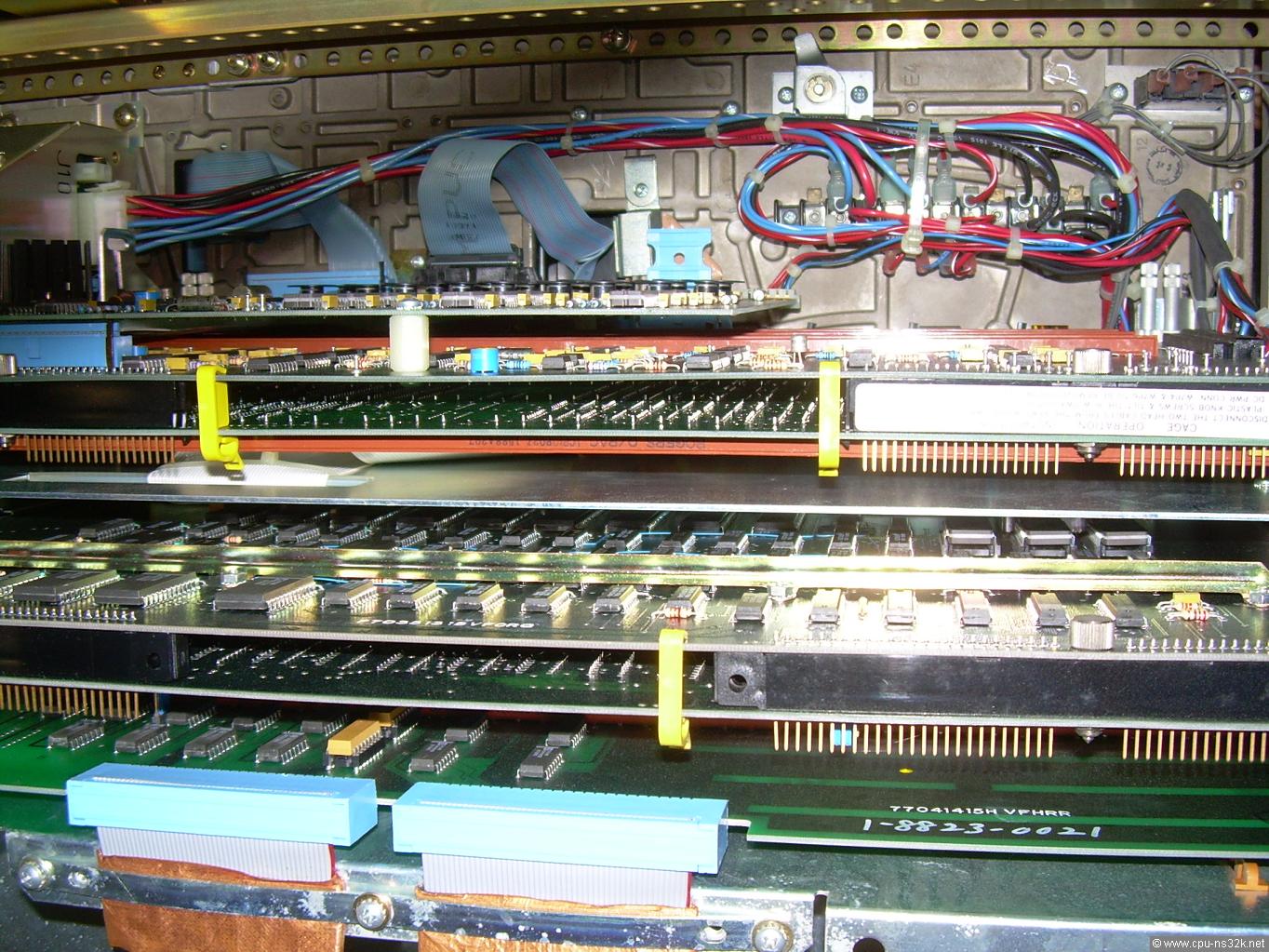
Fig. 39. The view of the electronic part for the tape unit is rotated by 90 degree. It shows a lot of stuff.
For me the Multimax is an impressive machine. And it would be sad if this machine is never running again. Therefore I plan for 2019 another visit of Jim's museum. This time I will have a mission: "wake up the beast!". I'm sure that I will need help for this demanding task. So everybody is invited to join me!
Hoststation 100
The Hoststation 100 was a user terminal with a 19 inch black & white monitor for the Multimax. In Figure 4 it is called the Asynchronous Hoststation R100. In the brochure in Figure 40 it is only called Hoststation 100. It has a serial interface and must be connected to the Annex Terminal Server.
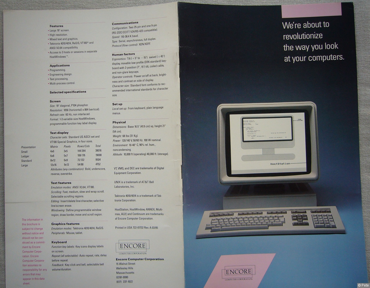
Fig. 40. A brochure about the Hoststation 100.
This terminal has an unusual horizontal resolution of 1056 pixel. This will make the logic more complicated. But the advantage for the user is more screen content which is more important. A mouse or a tablet could be connected to the terminal.
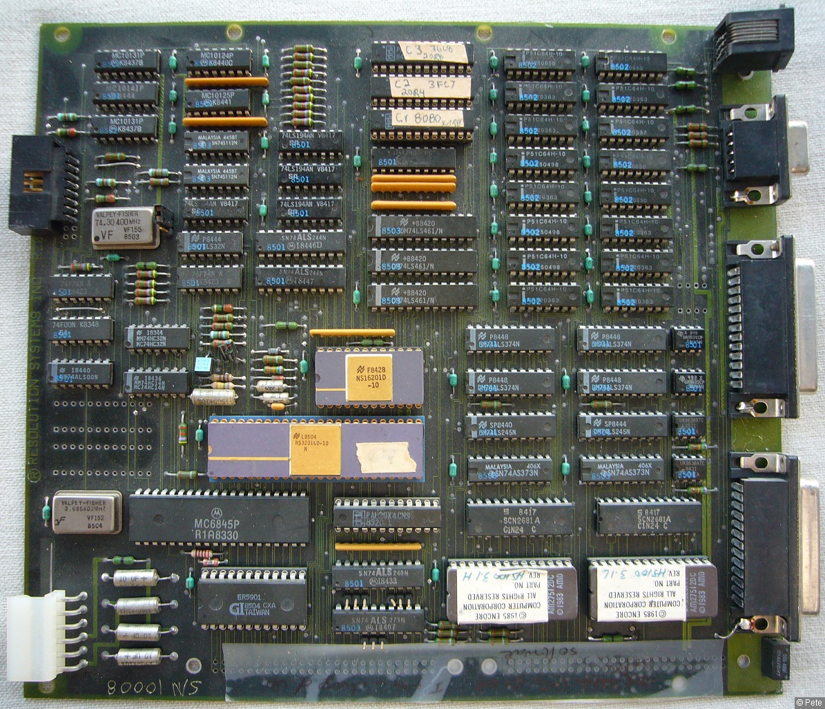
Fig. 41. The nice main board of the Hoststation 100.
The Hoststation 100 is based on an NS32016 CPU. Main memory is 128 kBytes of DRAM. The DRAM stores the screen content (1056 * 864 pixels = 114,048 bytes) and the working space (around 16.5 kByte) of the CPU. The board shown in Figure 41 uses 16 64 kbit DRAMs from Intel. The program store is made of two EPROMs of 64 kByte each.
The NS32201 TCU has no own quartz. I assume that the video clock of 74.304 MHz is divided by 4 for the TCU to make a CPU clock of 9.288 MHz. The advantage would be that the CPU is running synchronously to the video clock to avoid any disturbances of the sceen refresh.
In the upper left corner five ECL IC's of Motorola (MC10...) are placed. They are necessary because of the high video clock frequency. The DM74LS461 device in the middle is an 8 bit loadable counter. The package of the two UARTs SCN2681A is a 0.4 inch wide DIP. They can be found above the EPROMs. The standard video sync generator MC6845 is used.
I would really like to know whether this board is still functional. I have to discuss with Pete if he will allow me to apply power to it ...
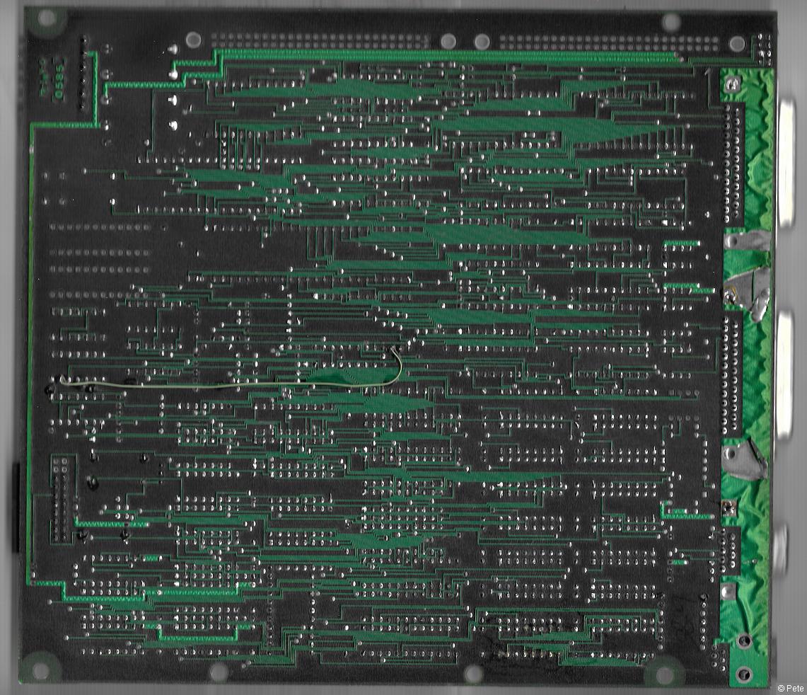
Fig. 42. The backside of the Hostation 100 main board. The layout looks like it was done automatically. Only one wire was needed to make this board functional.
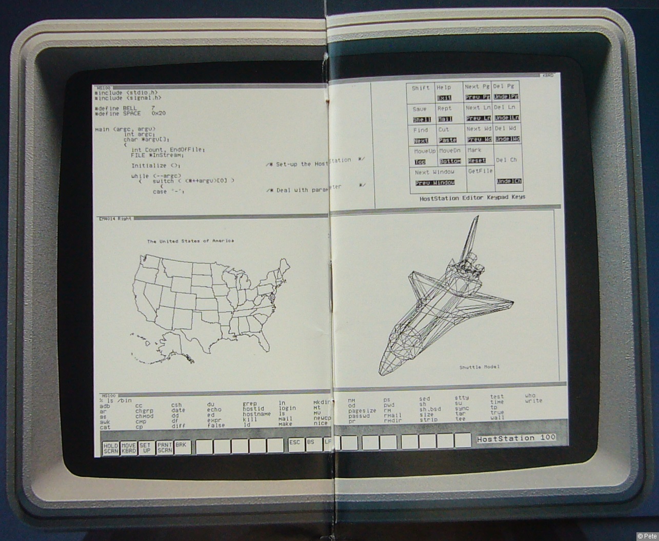
Fig. 43. The brochure shows some impressive screen shots of the black & white monitor. This one is my favorite (I'm fan of the Shuttle).
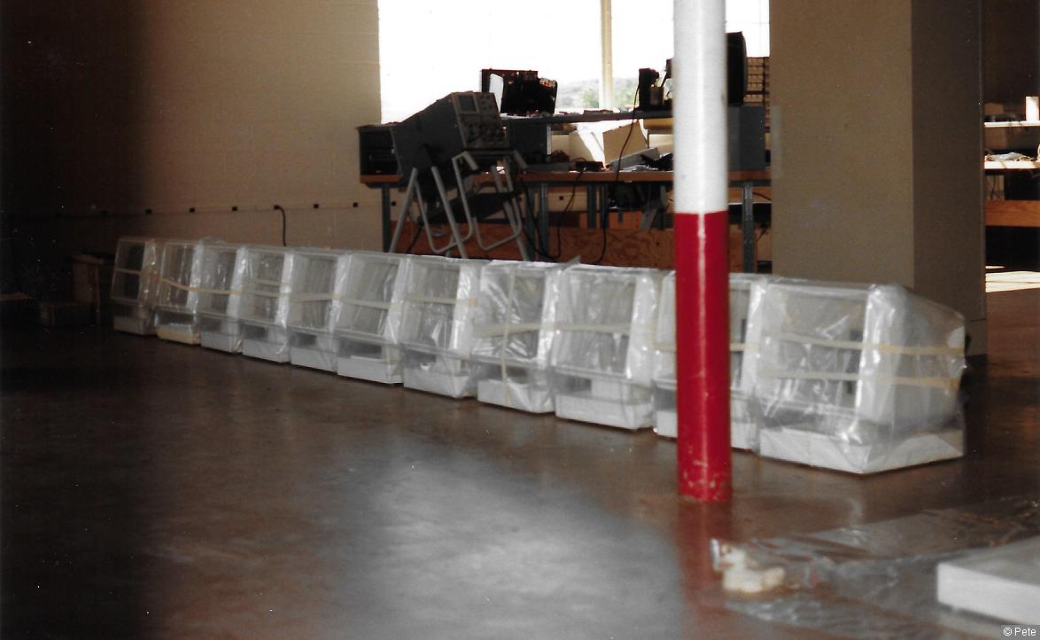
Fig. 44. This impression of the laboratory shows some cases of the Hoststation 100 at the floor.
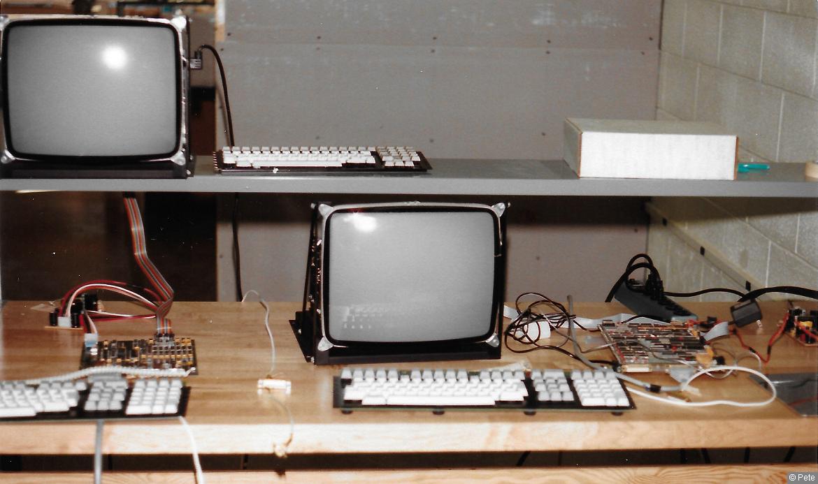
Fig. 45. Early versions of the Hoststation 100 being tested at the laboratory.
Thanks to Pete Lee who contributed to this chapter.
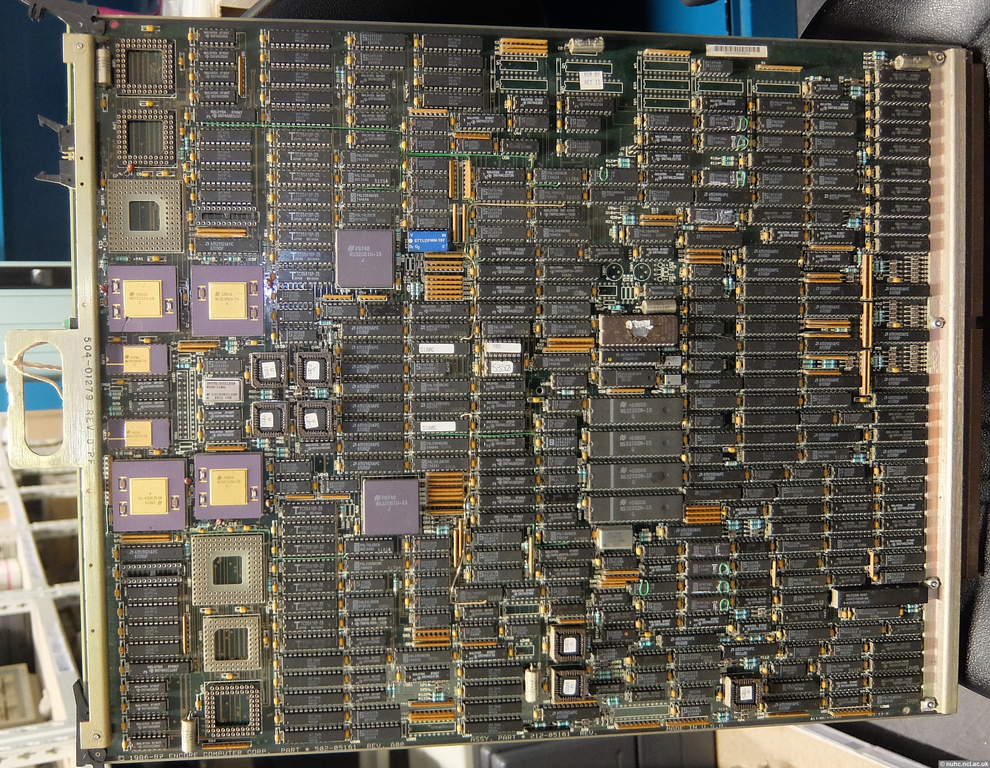
Advanced Dual Processor Card (APC)
In May 2025 Pete Lee sent me a photo of the CPU board APC. It is as impressive as the XPC board. The APC is build around two NS32332 CPUs running at 15 MHz.
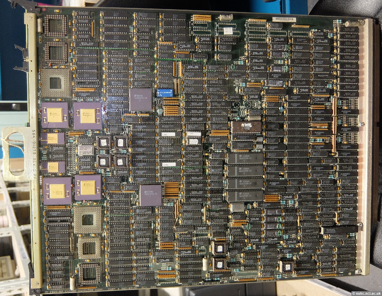
Fig. 46. Encore designed the most impressive Series 32000 boards. This photo is available in higher resolution here.
The six empty sockets are for two optional floating point accelerators. Each accelerator was made of three chips: one controller designed by Encore and two chips from Weitek which do the math. The Weitek chips are the WTL1164 and WTL1165, see their datasheet. The controller would also provide transcendental functions.
Unfortunately the Newcastle University did not buy the floating point accelerator option. I can imagine that this option was too expensive.
There is only one EPROM on the board. Maybe there was no space for a second one or Encore had a clever idea to share the content between the two CPUs. Noteworthy are the four ICUs NS32202 in the middle of the board. They support a lot of interrupts.
I would really like to see a circuit diagram of such a board. The people who designed it must be great engineers!
This chapter was last modified on 24 August 2025. Next chapter: Gary