Sequent Computer Systems
Sequent was founded in 1983 by former Intel employees. Their intention was to build computers based on SMP = Symmetric Multiprocessing. The idea was that a large number of microprocessors should be as powerful as a traditional mainframe. But the SMP system should be cheaper. This was a hot topic beginning of the 1980's because of the availability of 32 bit single chip microprocessors like Series 32000.
Sequent designed two systems based on NS32032: the Balance 8000 and the Balance 21000. The 8000 was the smaller system and could hold a maximum of 12 CPUs. The 21000 was the high-end system with a maximum of 30 CPUs. Both systems used a processor board with two CPUs and cache. A good description of the Balance 8000 can be found in the internet. More information about Sequent is available at Wikipedia.
I remember a story about the numbers of the Balance systems. The performance of an NS32032 was measured to 0.7 MIPS. Using 12 processors would result in a total performance of 8.4 MIPS. The bigger system with 30 CPUs has a performance of 21 MIPS. Multiply the numbers by 1000 and you get the system names.
The Sequent-Siemens AG Deal
In former times the Siemens AG built computers. These were expensive systems based on BS2000. Starting in the 1980's they looked for alternative architectures. There is rumor that Siemens AG was not able to design a system like the Balance on their own. But they want to offer something like this. The result in 1986 was a contract between Sequent and Siemens AG worth 50 millions US-$ which allowed Siemens AG to sell the Balance 8000 under their own brand.
The Balance 8000 became the MX500. It was the top product in the MX family - see the chapter Systems/Siemens for further details.
In October 2020 I got contact to someone who still owns some boards of an MX500. My first thought was to present the photos in the Siemens chapter. But obviously these boards were not made by Siemens. There is no printing on the board which indicates the manufacturer - very unusual if it were Siemens. But this is common practice in the OEM business.
Because I had no photo of any Sequent product I have put only a short hint in the chapter Systems/Multiple Vendors. With the photos it is time to make a chapter Sequent.
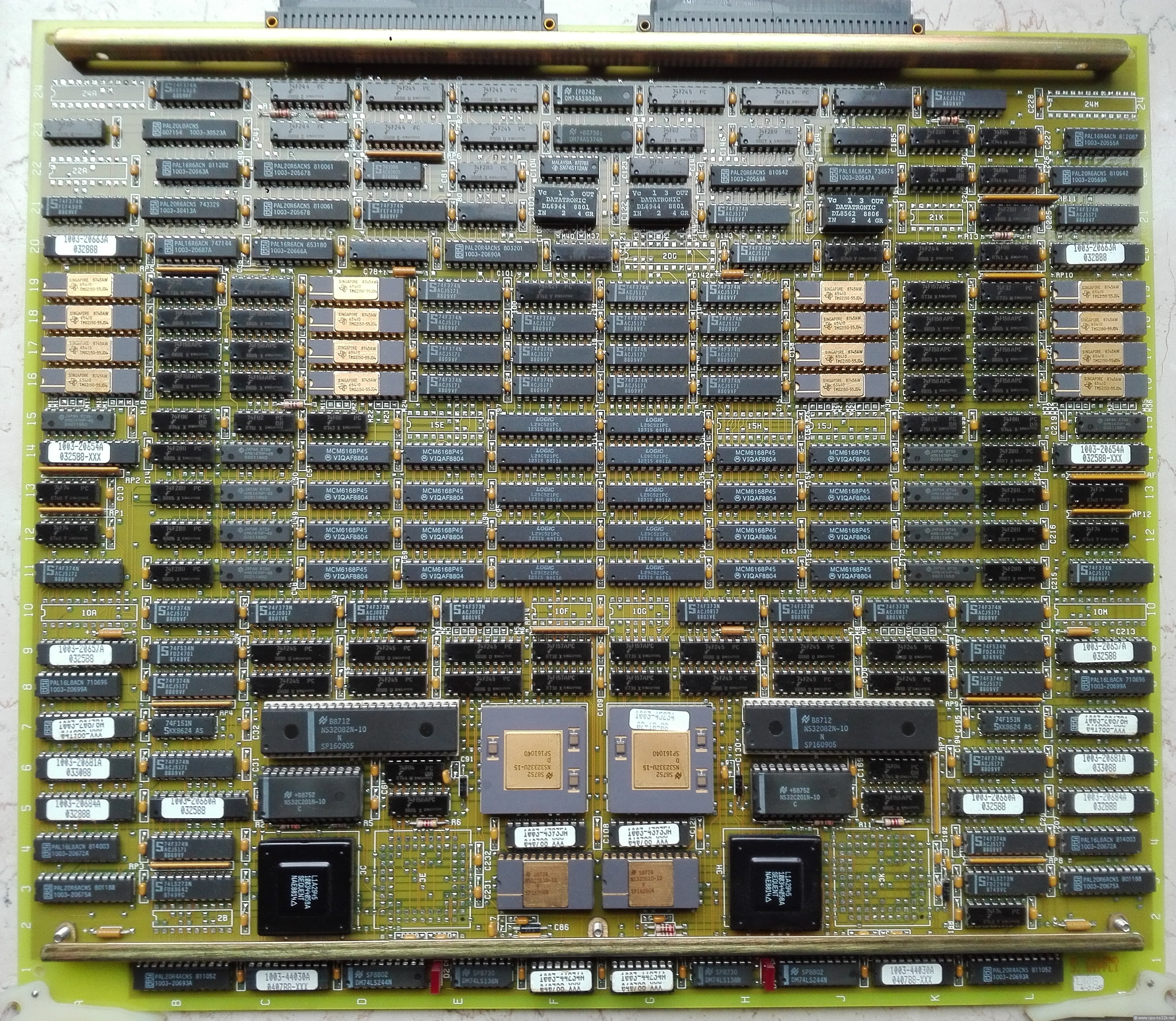
MX500 CPU Board
The owner of the boards was working as a programmer with one MX500 from the start until the machine was scrapped. He used the opportunity to save some boards and a disk drive - great job! I would have done the same :-)
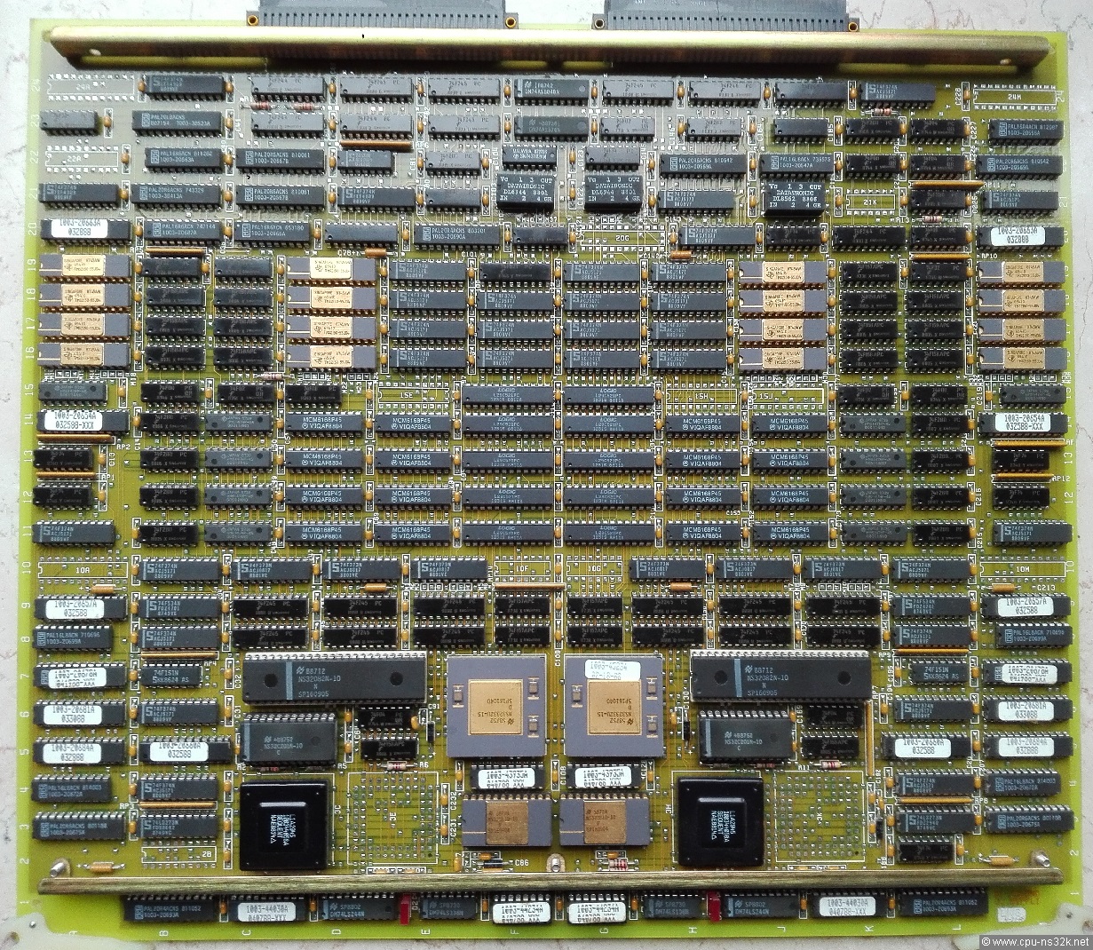
Fig. 1. The dual CPU board is build symmetrical: one CPU with their cache left, the other right. The bus connectors are at the top.
The above image is available in higher resolution: CPU. The size of the board is 360 mm * 310 mm.
The CPU board uses the 2nd generation CPU NS32332. At the same frequency as the NS32032 it delivers 50 % more performance. Although rated at 15 MHz the CPU cannot run faster than 10 MHz because of the maximum speed of the other members of the CPU cluster. They are the NS32081 Floating-Point Unit and the NS32082 Memory-Management Unit in an unusual plastic package. The clock generator NS32C201 has no external crystal. This could mean that the system has a central clock source which is possible at a clock rate of 10 MHz.
There is a 16 kByte local memory on the board for each CPU. It is build using eight MCM6168 4k*4 SRAMs. The memory is parity protected. The usual 74280 parity generator can be found near the one bit wide SRAM HM6147 which stores the parity bit. This is an important feature for a high reliability computer which will compete with mainframes.
8 kByte of the memory is used for local program and data. The other 8 kByte is used as a cache memory. The cache is organized as two way set-associative with a line size of 8 byte.
The cache tag memory is build with TMS2150. This memory is organized as 512 words by 8 bits. It contains an 8 bit comparator for address matching. Two TMS2150 are required to cover the full address range of 32 MByte. The first processor of the board was the NS32032 which has only an address range of 16 MByte. But the NS32082 MMU delivers the 25th address bit. The valid bit of a cache line can also be stored in the tag memory.
There are two groups of four TMS2150 for each CPU. The second group is necessary for bus snooping. This means that the external bus is permantently monitored for a write operation. If the write hits in the local cache then the entry is invalidated.
The cache replacement policy is that the oldest entry is overwritten. Therefore the cache must store which entry was last used. For this purpose a SRAM HM6147 is used. It is placed near the outer groups of TMS2150.
The Balance 8000 was build around a 12 slot bus backplane (another document says 9 slot - but this is in my view too little). Obviously Sequent learned from the first system that the number of CPUs can be increased without limiting the performance increase of each additional CPU. The result was that the Balance 21000 used a 26 slot (!) bus backplane. For me it is astonishing from an electrical point of view (bus load of each driver) and from a timing view. If every CPU is writing the average waiting time is 15 clock cycles!
But there might be a solution for this problem in the form of a write buffer for each CPU. There is an IC on the CPU board which I haven't seen yet and even the company was unknown to me: the L29C521PC from LOGIC. It's function is a 4*8 bit multilevel pipeline register. This chip can be used for a write buffer.
In the usenet archive I found an interesting remark about the power consumption of a Balance 8000:
"We have had some trouble due to an overloaded PSU in our Balance that caused some very strange errors that started to show up when we added more disks to it - seems the PSU isn't (wasn't?) designed to take 12 processors, 10MB of RAM, 2 Multibus adapters and a SCED card at same time.... It accumulates to some 200A on the +5V line, and the PSU is rated at 150A ..."
The owner of the boards told me another nice story about the opinion of the users of the Siemens MX500: "it is like a tractor - independant of the number of used terminals the computer was equal slow."
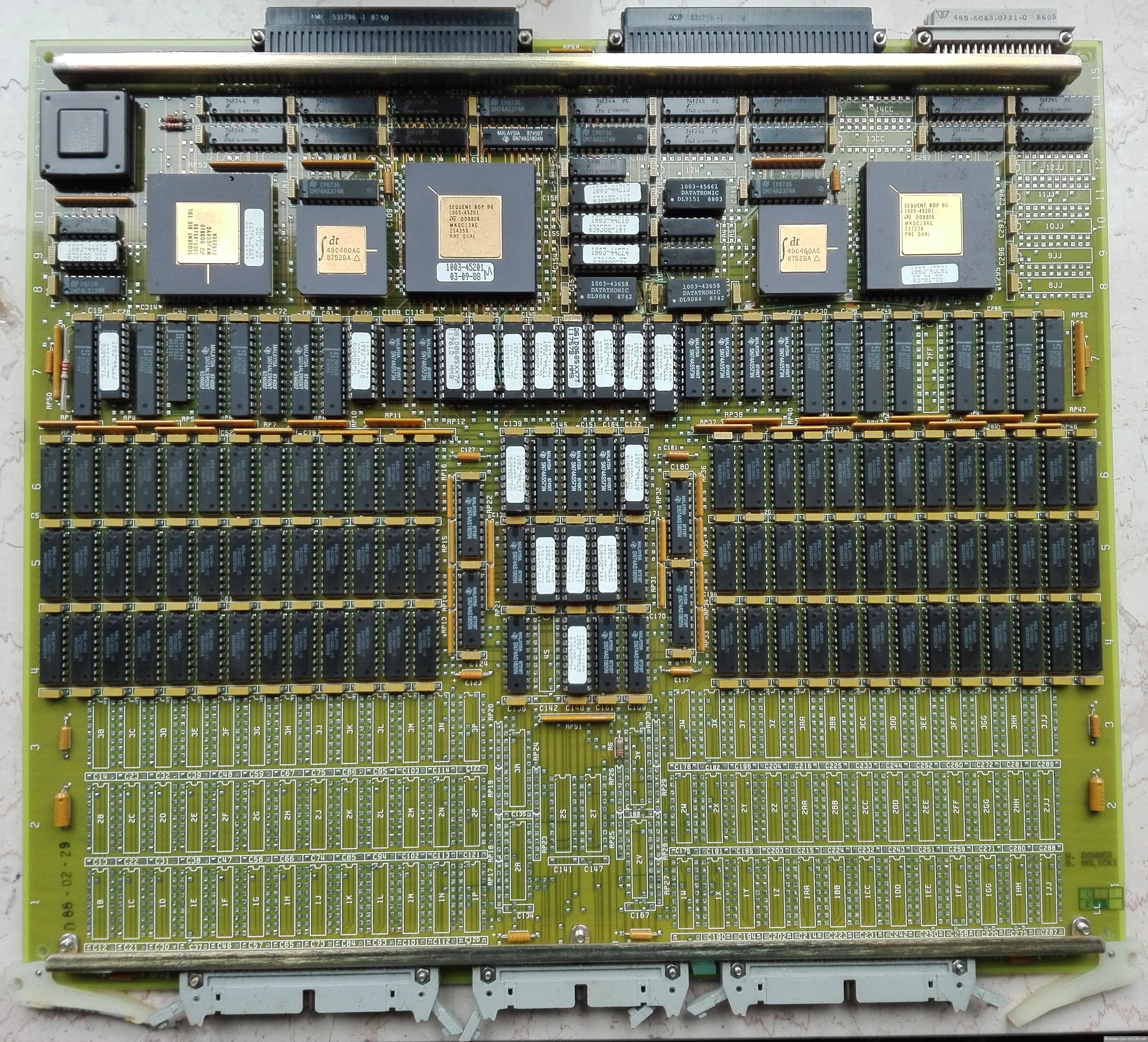
MX500 Memory Board
The standard building blocks of early SMP systems was the CPU board and the memory board. The customer could tailor the computer to his requirements with the number of used boards. If later he needs more performance or memory he could simply add more boards. This approach was very appealing to customers.
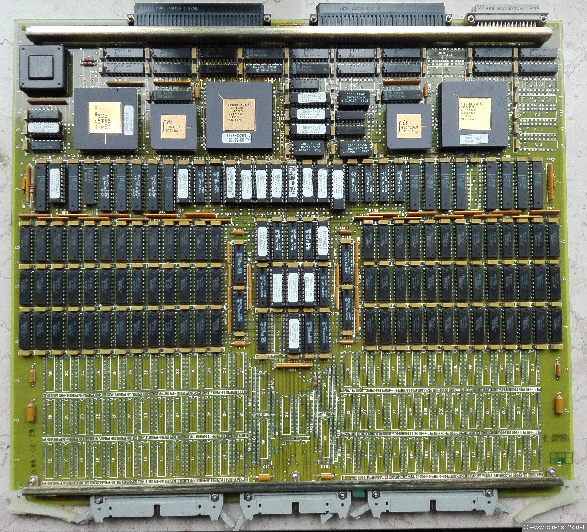
Fig. 2. This DRAM board of MX500 has 8 MByte of memory and space for another 8 MByte.
The above image is available in higher resolution: DRAM.
The DRAM is protected with the single-error-correction/double-error-detection (SECDED) chip from IDT, the IDT49C460. It needs 7 additional bits for protecting of a 32 bit data word. The board has two memory banks and therefore it has a total of 78 DRAMs of 1 Mbit each. The fact that 1 Mbit devices are used is an indication of the age of this board: no sooner than 1988.
There are three big ASICs on the board made by ST (SGS-Thompson). One is named SEQUENT BIC TDL and the other two are named SEQUENT BDG BG. I assume that they are used to buffer multiple accesses to the board.
The black IC in the upper left corner can also be found twice on the CPU board. This must be the ASIC for the "System Link and Interrupt Controller" (SLIC) bus.
The connectors at the lower edge are used for a local memory expansion. Why there is a third connector at the upper edge? No idea...
Software Aspects
Writing programs which use multiple processors to shorten the runtime are a demanding task. The operating system shall support the efficient execution of such programs.
I found in the internet a master thesis which describes "The concurrent environment of the Sequent Balance 8000". In addition the paper gives information about the required hardware for the concept of mutual exclusion. The master thesis is publicly available.
Next chapter: Siemens