Central Processing Units (CPUs)
| Device | Date | First Document |
|---|---|---|
| NS16032 | April 1982 | Preliminary Datasheet |
| NS16008S-6 | January 1983 | Preliminary Datasheet |
| NS32032-6 | August 1983 | Preliminary Datasheet |
| NS32032-10 | February 1984 | Preliminary Datasheet |
| NS32132 | 1986 | Preliminary Datasheet |
| NS32232 | 1984 | Series 32000 Databook |
| NS32332-15 | October 1985 | Preliminary Datasheet |
| NS32532-30 | October 1987 | Preliminary Datasheet |
| NS32CG16 | 1988 | Preliminary Datasheet |
| NS32CG160 | January 1992 | Preliminary Datasheet |
| NS32GX32-30 | May 1991 | Preliminary Datasheet |
| NS32GX320 | April 1991 | Preliminary Datasheet |
| Swordfish | March 1992 | Preliminary Datasheet |
| NS32FX16 | July 1991 | Preliminary Datasheet |
| NS32FX161 | February 1992 | Preliminary Datasheet |
| NS32AM16x | December 1992 | Preliminary Datasheet |
| NS32HT160 | June 1997 | No document available |
NS16032/NS32016/NS32C016
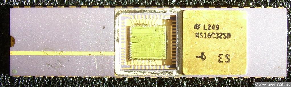
Fig. 1. The chip that should conquer the computer world: the NS16032 CPU.
The NS32016 CPU was the first implementation of the Series 32000 architecture. In the beginning the name was NS16032 but later National Semiconductor changed it to NS32016. The design of the chip started around 1980 and first reports appeared at the international solid-state circuits conference (ISSCC) in 1981.
The chip was build in a 3.5 µm NMOS technology. About 60,000 transistors were needed to implement the complex architecture including virtual memory support. The chip size was 7.4 mm * 7.4 mm = 54.76 mm² according to the report at ISSCC 1981. Speed selections of 6, 8 and 10 MHz clock frequency were offered. The package of the device was a 48-pin DIL ceramic package. With this low pin count only a 24 bits wide address bus multiplexed with a 16 bits wide data bus was available. Therefore the address space was limited to 16 Mbytes which was nevertheless huge for this time. An external access was done in 4 clock cylces. If the MMU was present in a system an additional clock cycle was needed for address translation. Then the available bus bandwith was 4 Mbytes/second at 10 MHz clock frequency.
The minimum instruction execution time was 4 clock cycles. This time was needed for all simple operations like ADD, SUB, AND, OR, XOR when both operands are in a register independent of the operand size which could be 8, 16 or 32 bits. MIPS was the very popular acronym for the description of the performance of a processor. The meaning is "million instructions per second". The NS32016 at 10 MHz achived a maximum of 2.5 MIPS. Obviously real world applications must load and store data from memory, do jumps and subroutine calls. This instructions need more clock cycles and therefore the so called "throughput" of the NS32016 is around 0.6 MIPS at 10 MHz clock frequency.
Unfortunately the first silicon of NS32016 had a lot of bugs. It is one thing to define a superior architecture on paper. But it is another thing to implement all the required functionality with a limited budget of time and man power. In addition simulation power in the beginning of the 1980's was very limited. Therefore the design team in Israel developed a new verification methodology called random testing. A random sequence of signals including interrupts and wait states was applied to the pins of the NS32016 and to a simulation model of the processor. If the output of the model and the real hardware is not identical there must be a bug either in the model or in the chip. Debugging the NS32016 took a few years from first silicon until the CPU runs succesfully Unix. This was one reason why the Series 32000 failed at the end.
In the beginning some critics mentioned that an 8-bit microprocessor, like the very popular Z80 or 6502, could outperform this 32-bit chip in certain tasks. For sure it is not useful to build a terminal with this high-end chip. But that was not the kind of applications the architecture was build for. The design team had data processing machines in mind and it was expected that advances in semiconductor processes will result in more powerful chips.
Later a CMOS implementation of the chip was presented. The NS32C016 achieved 15 MHz clock frequency and used much less power.
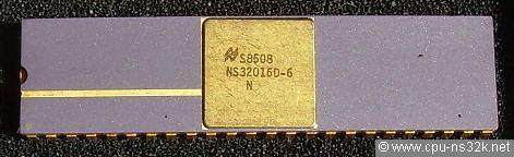
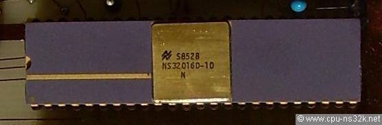
Fig. 2/3. The NS32016 CPU specified for 6 MHz (left) and 10 MHz (right) operation.
The golden cap of the package shows more than the product name. My assumption is that right from the National Semiconductor symbol is the date code. S8508 on the left NS32016 can be translated to "being produced in 1985 in the week 08". On other chips you can see a wafer code or something similar. The N is most probably the design step.
Fig. 4. The NS32016 CPU in a plastic package.
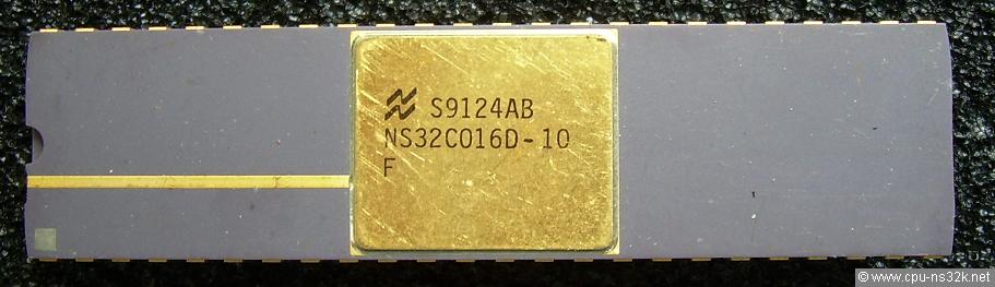
Fig. 5. The first CMOS CPU: the NS32C016. The golden cap is bigger than the cap of the NS32016.
NS16008/NS08032/NS32008
The NS08032 was an NS16032 with an 8 bits wide external data bus. All characteristics of the Series 32000 architecture have been implemented with the exception of virtual memory support. This feature makes no sense with a narrow 8-bit data bus. This chip should allow customers to build cheap computers which are able to run the same software like the faster and therefore more expensive machines. The package and pin-out of this device was identical to the NS16032 CPU.
Although the CPU used 8 bits for the data bus the slave processor interface was 16 bits wide. This feature improved the available bus bandwith between CPU and FPU.
I don't know when the NS16008 was renamed to the NS08032. Figure 6 shows a german advertisement of National Semiconductor which uses the new name. NS08032 is a more logical name compared to NS16008. But how do you recognize this device as a member of the NS16000 microprocessor family? The same problem existed for the NS32032. The solution was to rename the NS16000 family to Series 32000.
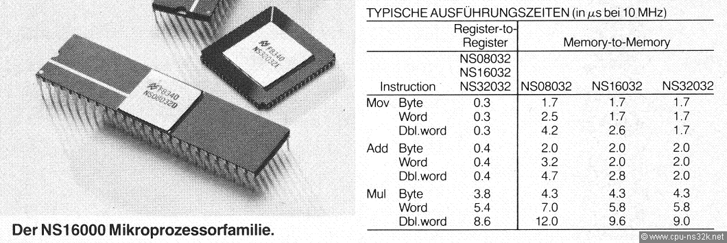
Fig. 6. The NS08032 CPU had a short live.
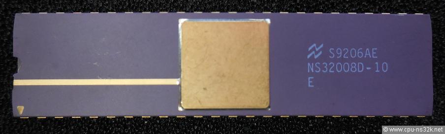
Fig. 7. An NS32008 CPU from 1992 rated at 10 MHz clock frequency. It is unusual that the marking is not on the lid.
Gilbert sent me a photo of his NS32008 in May 2017, see Figure 7. He said that this device is still available at ebay.
NS32032/NS32C032
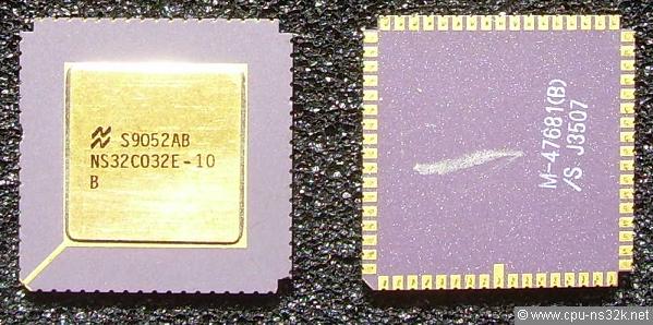
Fig. 8. The NS32C032 CPU specified for 10 MHz operation.
The NS32032 CPU was the third CPU version of the first generation Series 32000 chips. The difference to the NS32016 was a 32 bits wide multiplexed address/data bus. The address bus was still 24 bits wide like the NS32016 and used the lower part of the 32-bit bus. The package was a 68-pin leadless chip carrier. Maximum operating frequency of the NMOS chip was 10 MHz. Surprisingly a datasheet exists which describes a 4 MHz version of this chip. Some time later a CMOS implementation (NS32C032) was presented with 15 MHz maximum operating frequency. This version was also available in a plastic package (68-pin PLCC) due to its low power consumption.
The performance gain compared to the 16-bit version NS32016 is very well documented in the Application Note AN-464. Between 7% minimum and up to 40% maximum was the NS32032 faster according to these benchmarks. Also in this document National Semiconductor said both processors are internally identical except in the instruction fetch queue and the bus interface. At the end a lot of systems were designed for the NS32032. Some of them were highly sophisticated multiprocessor machines.
NS32132
To get an advantage from systems using a 32 bits wide data bus a NS32132 was announced. Two of this chips could be tigthly coupled for a multiprocessor system. This was possible because a single NS32032 could not consume the available bus bandwidth which is 8 Mbytes/second at 10 MHz. If it is only 50% you can add a second processor to the bus with no disadvantage. The assumption of 50% is obvious if you consider that the NS32016 CPU is optimized for a 16-bit data bus and should therefore consume nearly 100% of the bandwidth.
Three reserved pins of the NS32032 were used for special control signals to simplify system design. E-LAB was using this approach and was the only one I know. Soon the NS32332 was a better alternative for building powerful 32-bit computers. In the 1988 edition of the Series 32000 family databook the NS32132 is no longer described.
But if you look into the datasheets of NS32032 and NS32C032, which were printed after the time when the NS32132 disappeared, the three pins are described as if the dual-processor function is still in. Also the die photo of NS32032 shows that the three pins have bond wires. Therefore I plan to make a test board with two 68-pin sockets and then see what happens...
NS32232
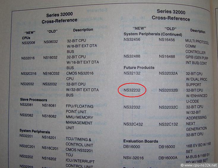
Fig. 9. The one and only hint for an NS32232 CPU can be found in the 1984 Series 32000 databook.
The NS32C432 in Figure 9 became the NS32532.
In June 2024 I got a mail saying that U-CODE means microcode, not user code as I have thought. Today it is standard to use the letter "µ" to say that something is "micro". But in the 1980's this letter was not available on keyboards and "u" was used for this purpose. Technically it makes sense to enhance the microcode of the NS32032 to make more use of the 32 bit data bus. Thank you for this hint!
NS32332
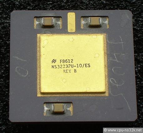
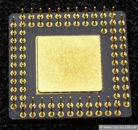
Fig. 10/11. This early version of the NS32332 CPU is an "/ES" = engineering sample. The pin A1 identifier is the additional pin in the upper right corner of the right picture.
The NS32332 CPU was the second generation of the Series 32000 family and appeared around 1986. This chip had for the first time in the Series 32000 family a full 32-bit address path. This enables access to 4 Gbytes which was quite a lot for the middle of the 1980's. Again address and data were multiplexed over the same pins. An external access was done in 4 clock cycles independent of the MMU doing address translation. A new feature was added called "Burst Cycles" which required only two clock cycles per fetch. The maximum bandwith was (16 Byte) / (4+2+2+2 clock cyles) = 24 Mbytes/second at 15 MHz. In addition the chip had some internal enhancements like a deeper instruction buffer and a separate address adder.
The chip was housed in an 84-pin PGA package. Approximately 80,000 transistors were placed on a die which measures 10.1 x 8.7 = 87.87 mm². It was implemented in a 2.8 micron NMOS technology with a single metal and a single poly layer. The maximum clock frequency was 15 MHz. At this frequency the NS32332 was 2 to 3 times faster than a NS32032.
NS32532
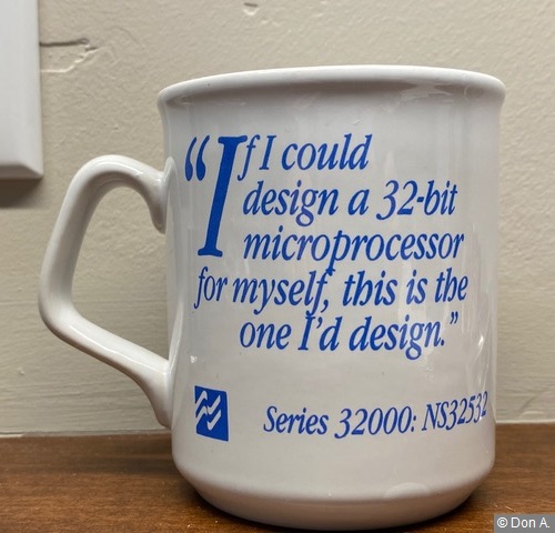
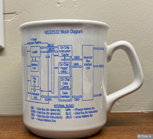
Fig. 12/13. A former member of the design team sent me the photos of a special cup. I would also like to have such a cup :-)
The NS32532 CPU was the third generation of the Series 32000 architecture. The design was a big step forward. Due to the advances in process technology 370,000 transistors could be integrated. This was enough to integrate three functions for the first time: an instruction cache, a data cache and the memory management unit. The caches needed 130,000 transistors (25% of die area) and the MMU 30,000 transistors (10% of die area). Figure 13 of chapter Chips/Die Photos shows the NS32532 die with the overlayed block structure.
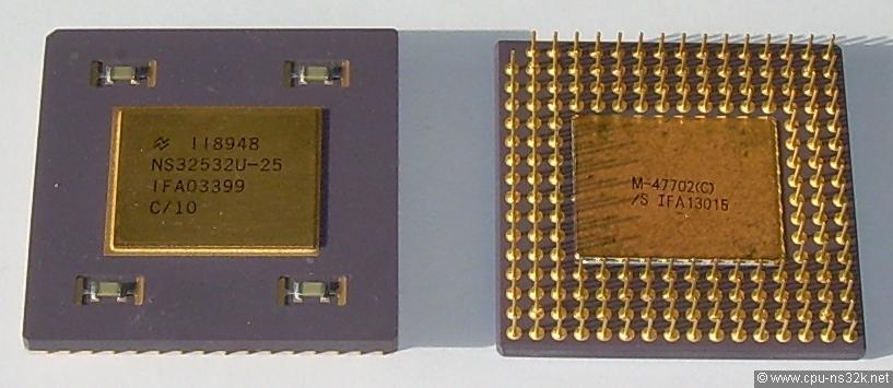
Fig. 14. Frontside and backside of the NS32532 CPU specified for 25 MHz operation.
The first silicon of the CPU was build in a double-metal 1.5 µm CMOS technology achieving 20 MHz. It appeared in 1988 on the market. The final version used a shrinked 1.25 µm CMOS process which allowed higher clock speeds of 25 and 30 MHz.
The package was a huge 175-pin PGA. This high pin count was necessary to separate the 32 bit address and data busses. National wanted to improve performance. But there is doubt that separate busses are really helpful. The caches had 1024 bytes for data and 512 bytes for instruction. This is not much but my own experience showed that switching them off degrades performance signifcantly. The external accesses became much faster compared to the NS32332. The bandwitdth was now (16 Byte) / (2+1+1+1 clock cycles) = 80 Mbytes/second at 25 MHz. This is a 20-fold improvement compared to the NS32016!
The integrated MMU contains now a 64 entry fully associative translation look-aside buffer (TLB). This is twice as much as the TLB had inside the NS32382 and NS32082 MMUs. The reason behind this decision is that programs and data structures are constantly growing in size. Register definitions and debug capabillites changed once again compared to the NS32382 MMU. The debug register were now part of the CPU register file (access by LPR/SPR instead of LMR/SMR).
Instruction execution time was now a minimum of 2 clock cycles. With the help of the caches and improved pipelining this was even true for instructions which have one source operand in memory. The maximum MIPS rating for a 30 MHz NS32532 was 15 MIPS and the real world value could easily approach 10 MIPS. This is over 10 times more througput than the NS32016!
The design team in Israel had gained a lot of experience since the first silicon of the NS32016. Their random testing proved to be very successful. The first silicon of NS32532 was able to run UNIX!
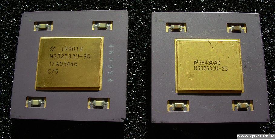
Fig. 15. Two more NS32532 of my collection: one 30 MHz device (left) and the other very young device (right).
In October 2015 I saw for the first time an NS32532 specified for 30 MHz clock frequency - thanks to Pauli! I tested the CPU at 25 MHz for one hour in my PC532E system - no problems! The device was obviously not handled with care. Some ceramic broke away in the lower right corner and at the upper edge.
But there is a certain question: where is the system gone that hold this CPU?
The right device in Figure 15 is the newest NS32532 I have. Its datecode is S9430AD which is KW30 of 1994. Also the new logo of National Semicondutor is used. Interesting to note is the missing steping code.
A former design engineer of National Semiconductor wrote about the development of the NS32532:
"From my perspective the NS32532 was designed at an interesting intersection in time where new CAD tools had to be rapidly developed so as to allow for development of large CPUs. Therefore at NSTA, and specifically for the design of the 532, tools were developed internally to support the effort. One was called Z that allowed for the development of the chip and its simulation using Boolean algebra. This was a departure from the schematic capture, where engineers used to design by placing actual logic gates (NANDs, NORs, FFs, etc.) we simply wrote equations. To allow the more veteran engineers who were used to checking circuits viewing the schematics, a tool was developed that transformed these equations into a drawing. It was called SHELED (skeleton in Hebrew) but was an acronym that I cannot recall."
NSTA was the name of the design center and the acronym for National Semiconductor Tel Aviv .
NS32CG16
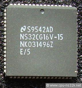
Fig. 16. The NS32CG16 CPU specified for 15 MHz operation.
The NS32CG16 CPU was a special development for the printer market. This CPU was similar to the NS32C016. Major changes were the lack of virtual memory support and an enhanced instruction set with 11 additional instructions for graphics applications. To lower system costs the functionality of the NS32201 TCU was integrated. Maximum clock frequency was 15 MHz. The package of the device was a 68-pin PLCC.
David Rand was a member of the NS32CG16 developer team. Before joining National Semiconductor he worked for Definicon on the development of the first PC coprocessor board, the DSI-32 (see Systems/Definicon). He wrote about his time at National Semiconductor:
"All of the CG16 development was done in Santa Clara. Haluk Aytac, Mo Reddy, Amos Ben-Meir and I worked on the microcode. Most of the original CG16 code was done by Haluk and Mo - I came to the party a couple of months after the project started, but well before the first silicon was made. Much of my time was spent doing simulation runs to get execution timing, and to look for bugs. The simulator was run on a DEC cluster, and was really, really slow. Most of the simulations only lasted a few hundred clocks, but took many, many hours of real-time.*)
The first silicon did not work. There were some internal pull-ups that were not connected. So, we used a probe station, micro-probes and several packaged parts to explore the functionality. We did get it to work. As I recall, three probes were required - and since we were doing this in a lab in the "marketing" building on Kifer Road, the probes would occasionally skitter over the die and then we would have to use a new chip :-)
Some of the other notable design changes were to fix a metastable condition in the interrupt line. If interrupts were not synchronous to the clock (and what interrupts would be?), the chip would lock up in unusual states. The final silicon fixed this.
The power-down features of the chip were neat, too - allowing you to dynamically change the clock divisor. I found that really interesting for the 32k line.
All in all, I really enjoyed working on this part, and was quite happy that it found a home in the printers of the late 80's."
*) This was a digital simulator for microcode development. My own experiences with VAX machines tell me that David's jobs may have gotten a low priority ...
David sent me a special highlight: a piece of Series 32000 microcode. The instruction shown in Figure 17 was present in the original NS32CG16 but was deleted to save space in the final version. The ROTIMG allowed for rotation of an 8x8 image by 90 or 270 degrees. David remembers some sleepless nights designing the algorithm.
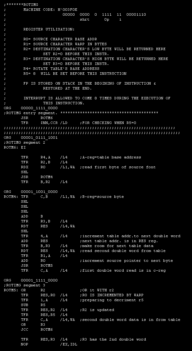
Fig. 17. A piece of microcode for the NS32CG16 - up to now the only piece I have seen!
Each line of the microcode is executed in one clock cylce. I asked David for some documentation about the microcode. But he answered that there was none. Or he never found it. Information was passed directly from the other engineers.
Maybe there was something written in Hebrew because the NS16032 was developed in Israel. And nobody ever translated it to English.
NS32CG160
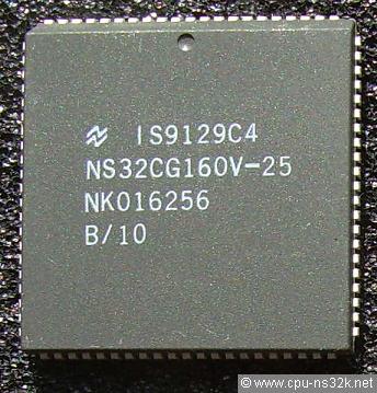
Fig. 18. The NS32CG160 CPU specified for 25 MHz operation.
The NS32CG160 CPU was a faster version of the NS32CG16 CPU with additional peripherals on chip. Further enhancements were the support of the Direct-Exception mode and a 16 * 16-bit hardware multiplier. Maximum clock frequency was 25 MHz. The package of the device was a 84-pin PLCC. Despite the higher clock frequency and the mentioned enhancements the CPU was identical to the original NS32016 CPU design. This can be verified by comparing the instruction execution times.
To lower production costs the chip was built in a modern 0.8 μm CMOS technology.
NS32GX32
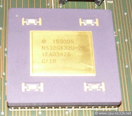
Fig. 19. The NS32GX32 CPU specified for 25 MHz operation.
The NS32GX32 CPU was a simple cut down of the NS32532. Only the virtual memory support (mainly the MMU) was taken out. Whether this was a complete chip redesign or just NS32532 chips with a defect MMU is not known to me. The CPU went into embedded designs like laser printers. The ETH Zürich used this processor for the CERES 3 workstation.
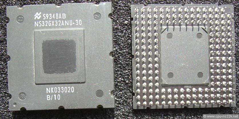
Fig. 20. The "A" version of the NS32GX32 CPU in an unusual plastic PGA.
Figure 20 shows a version of the NS32GX32 CPU in a cheap plasic package. This was the first time I saw a plastic version of a normally ceramic PGA package. The package uses two identifiers, "N" for plastic and "U" for Pin-Grid-Array (PGA). The name of the device (NS32GX32A) may indicate modifications of the original NS32GX32. Since December 2019 I know that the "A" version has a reworked chip layout and uses the 0.8 μm technology.
NS32GX320
Due to the success of the NS32GX32 in the laser printer market the successor NS32GX320 was build which integrated more functions and offered an enhanced instruction set. The integrated functions were a 2-channel DMA controller, a 15-level interrupt control unit (ICU) and three 16-bit timers. In addition some instructions need less clock cycles to execute. The chip was fabricated in a 0.8 μm CMOS technology. Surprisingly this 50% shrinked process didn't deliver chips with a higher clock speed than the NS32532. Top speed was still 30 MHz. The number of transistors was 390,000 which is 20,000 more than the NS32532. It would be interesting to see a die photo of this device!
In 2019 I tried to get one from a chinese reseller. But the price of 300 US-$ was too high...
The device used the plastic PGA package shown in Figure 20. Although the number of pins was unchanged compared to the NS32GX32 the devices are not pin compatible.
Four new instructions were added. Three of them perform a multiply-accumulate operation and the fourth one is a special form of multiply. All four are very useful in DSP applications.
Swordfish
The Swordfish CPU was the most advanced design of the Series 32000 family. Mark Smotherman from the University of Clemson in South Carolina wrote a very good article about the chip. I got his permission to present the article here.
Some more information about Swordfish can be found in a presentation at the conference Hot Chips 3 in 1991:
![]()
Fig. 21. National Semiconductor was proud of the product: the Swordfish logo.
For me the product name was NS32764. I learned about a planned design in May 1988 from the german electronic newspaper "Markt & Technik". I still have a copy of the page. Little was said but it should be a RISC design and as a special feature it would be 100% software compatible to Series 32000. I remember being disappointed that also National Semiconductor jumped on the RISC train. I could not imagine during this time how a powerful Series 32000 processor could come out of a RISC design. Today every child knows that the old CISC architecture x86 gets its power from an internal RISC design.
In August 2015 I learned that Swordfish got a different product name. On the logo in Figure 21 you can see NS32SF640. It requires no great thought to decode SF as being a shortform of Swordfish. But there is also an NS32SF641. You find the name on the photo in the chapter Chips/Die Photos. According to a text of the Computer History Museum the NS32SF640 is a "64-bit CPU without FPU" and the "NS32SF641 has integral FPU". I guess that the NS32SF640 has a non-functional FPU. According to the presentation at the Hot Chip conference Swordfish must have had an impressive floating point performance even surpassing the famous Weitek coprocessors.
Also at the Computer History Museum I found a photo of an NS32SF640. You can see it in Figure 22. Regarding the size of the lid the die must be huge.
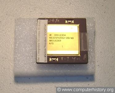
Fig. 22. An NS32SF640 in a museum. Is it the only survivor?
Swordfish has an external 64 bits wide data bus. This leads to the "640/641" in the product name. The resulting bandwith is a must have for superscalar CPU designs. The drawback is a bigger board size. An example of it is shown in the Figure 23.
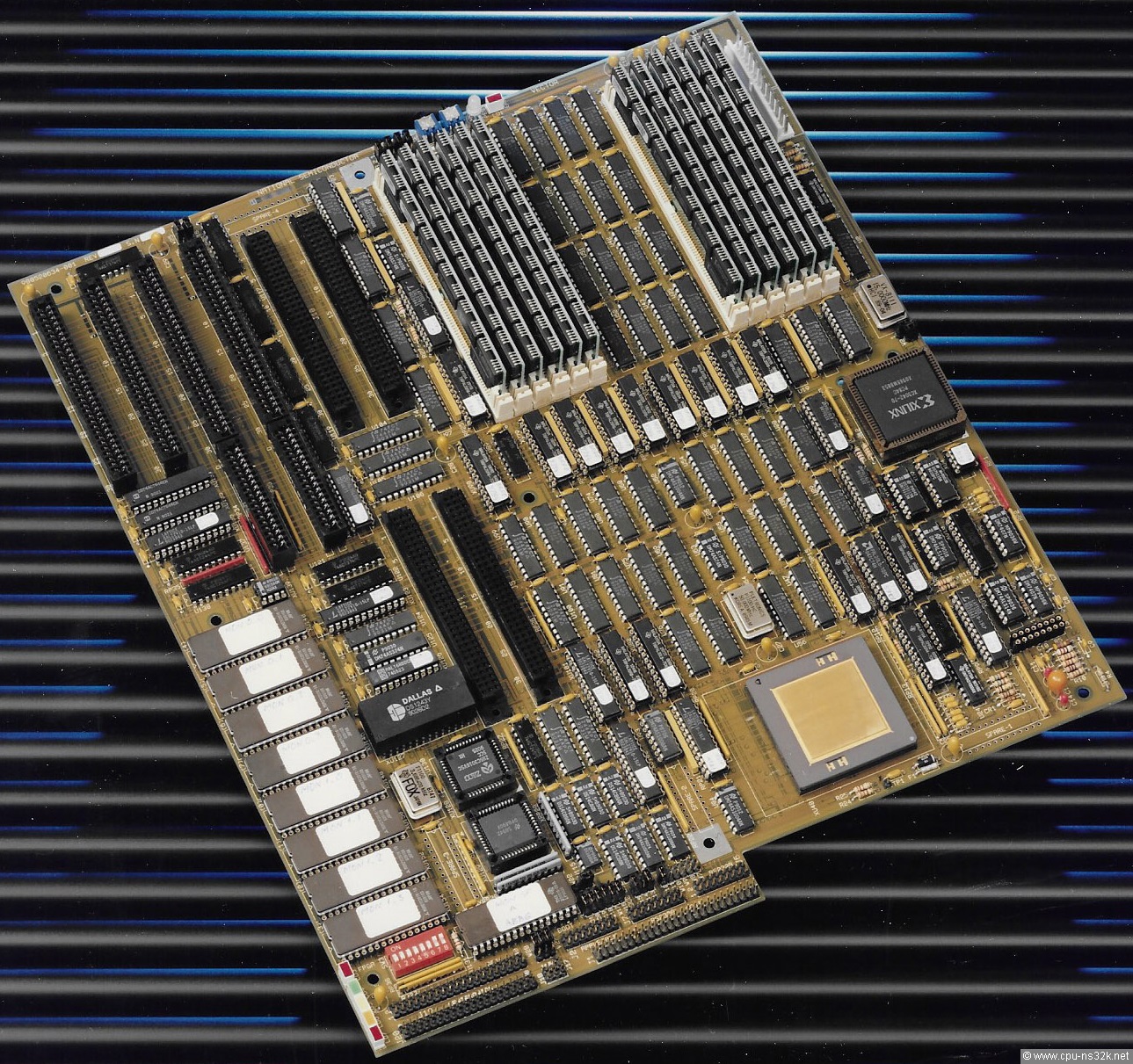
Fig. 23. A big development board of National Semiconductor for Swordfish.
The board was used for software development. The RISC design of Swordfish was new and therefore new programs had to be written. Of course National Semiconductor could use the old Series 32000 tools to test first silicon. But I think the engineers were excited to see their RISC design running.
The Swordfish on this board has no marking and misses the capacitors on the package. Maybe it is only a mechanical sample. Although Swordfish has a 64-bit data bus the package has only two capacitors on it. The NS32532 has a 32-bit data bus but its package contains four capacitors. At the upper edge is a device from Xilinx which might be an FPGA. The organization of the DRAM looks like two banks with six standard DRAM modules per bank. Each bank can deliver 32 bits of the data bus. If 4-MByte modules were used total memory was 48 Mbytes. Interesstingly there is a bank of 8 EPROMs at the lower left edge of the board. Either Swordfish does not support dynamic bus sizing like the NS32532 or it was not functional ...
Unfortunately I could not find a datasheet of Swordfish until now. But I will not give up!
Swordfish Part 2
In October 2020 I got a lot of new stuff, especially about Swordfish - thanks a lot to Don Alpert, Alon and Roberto!
Finally I can present the photo which showed me for the first time that a datasheet of Swordfish exists - see Figure 24.
Fig. 24. A lot of datasheets and manuals but one of them is very special - the preliminary datasheet of NS32SF641 ! The search is over :-)
The cover pages of the datasheet are available here: cover pages
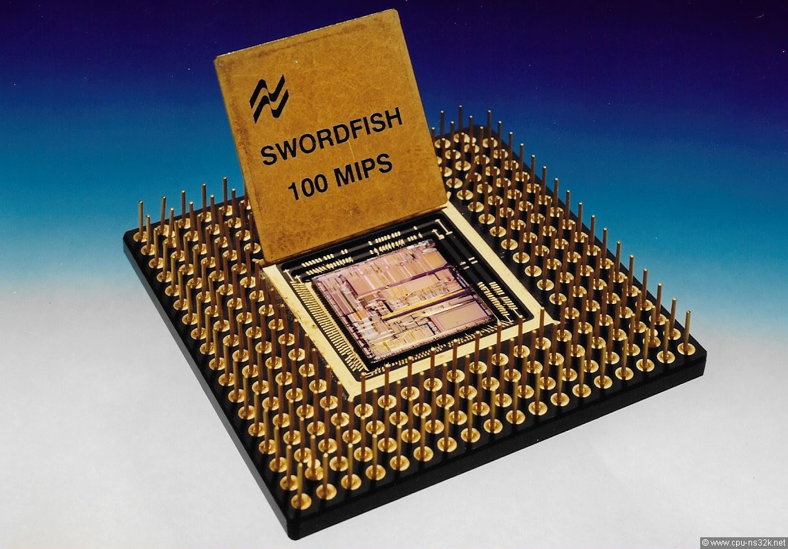
Fig. 25. Swordfish was build into a PGA package with 223 pins due to its 64 bit wide databus.
The pages of the datasheet which contains the pin description are available here: pinout (zip file)
I got two documents from National Semiconductor about Swordfish: one is the News Release of February 1991 and the other is a Backgrounder.
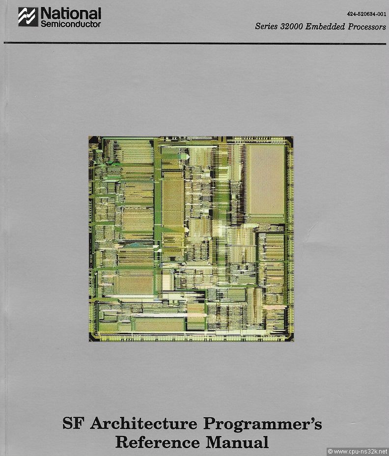
Fig. 26. The image shows the front cover of the S(word)F(ish) Architecture Programmer's Reference Manual.
The list of content of the Reference Manual is available here: Contents
There is an interesting statement on the front cover of the preliminary datasheet: "The NS32SF641 and the NS32SF640 are software compatible with other microprocessors in the same family."
I don't know on which assumptions this statement was made by National Semiconductor. For me software compatibility is given if one microprocessor can execute the binary code of another microprocessor. But a look in the list of content shows a fully different instruction set compared to other Series 32000 members!
Therefore in my view Swordfish is no Series 32000 processor. But it is definitly part of the Series 32000 story!
NS32FX16
Fig. 27. The sad fate of a great architecure: being the processor of a fax machine.
After National Semiconductor found out that it has no chance to be succesful in the workstation market (despite Swordfish) they entered the embedded processor market. The Series 32000 found home in such exciting products like printers, fax machines and answering machines.
The NS32CG16 device for the printer market was the first result of this strategy change. The company Canon of Japan - the number 1 printer manufacturer at that time - was the first customer to use this chip. The NS32CG16 became the basis for all following application specific devices.
The second device of the new line was the NS32FX16. It was build for fax applications. This device implemented for the first time ever a combination of a CPU and a Digital Signal Processor (DSP) on one chip. The interface to the DSP is a memory-mapped register set. After initializing by the CPU the DSP works on data from external memory and the on-chip memory. During this time the CPU is free to do other tasks. The on-chip memory of 384 bytes can be accessed either by the CPU (read/write) or by the DSP (read only). The main task of the DSP accelerator was the modem software of a fax machine. Maximum clock frequency of the device was 25 MHz. For this speed an external crystal of 50 MHz was required. It was fabricated in 1 µm CMOS technology and was packaged in a 68-pin PLCC.
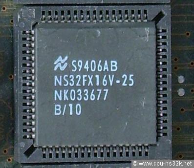
Fig. 28. The NS32FX16 CPU in a socket of an Indel AG board.
NS32FX161
The NS32FX161 was an improved pin compatible version of the NS32FX16. The DSP was more powerful and the RAM was expanded to 4 kbytes. This enhancements supported higher modem speeds. The CPU core implemented the Direct-Exception mode of the NS32532 for faster interrupt processing. A CMOS process with 0.8 µm feature size was used for this device.
NS32AM16x
The NS32AM16x products were based on the CPU core and the DSP of the NS32FX161. The on-chip RAM size was 2.1 kbytes. New for any Series 32000 product was the integration of up to 32 kbytes of ROM. This processors were used in small sized digital answering machines. Therefore they integrate nearly everything of this application. Also a subset of the NS32202 ICU was included. Today such a device is called a system-on-a-chip and many of them are available for all kind of applications. But beginning of the 90's the NS32AM16x were one of the first of its kind.
The NS32AM16x had an interface for 4-Mbit and 16-Mbit DRAM. The DRAMs of answering machines have more defects than can be repaired with on-chip redundancy. Therefore this DRAMs cannot be sold as computer memory. But for speech applications it doesn't matter if some bits are failing. One other main part of an answering machine is the CODEC. It converts analog voltages to digital values and digital values to analog voltages. The NS32AM160/161 were connected to CODECs with a parallel interface and for CODECs with a serial interface the NS32AM162/163 were used. All versions had a fixed clock frequency of 20.48 MHz and a 68-pin PLCC package.
Somehow strange was the BITBLT capability of the devices. There is obviously no need for this in an answering machine. But the effort to take it out was not worth the saving. Even changeing a running testprogram in production means effort and if there is no higher yield (= number of good chips) you better skip it.
NS32HT160
The NS32HT160 was an ASIC development with silicon available in 1997. ASIC = "Application Specific IC" means that the chip was made for a certain customer. In this case the CPU was used by France Telecom for a videotext terminal (Minitel 4).
The NS32HT160 has a CPU and a DSP similar to the NS32FX16. In addition it controls a Video-RAM to support display functionality. Figure 28 shows the CPU board of a Minitel 4 terminal. The HM538253BJ-7 from Hitachi is a 2-Mbit VRAM organized 256k x 8bit with a 512 x 8bit shift register. A ROM from Samsung and a DRAM from NEC is placed on the bottom side.
Fig. 28. The NS32HT160 is the heart of the Minitel 4 videotext terminal. Thanks to Hervé for this discovery!
The NS32HT160 is packaged in a 132-pin TQFP. It is specified for 20MHz operation. The chip seems not to have any ROM inside. Therefore it would be a nice chip to play with if something like a datasheet can be found...
This chapter was last modified on 24 June 2024. Next chapter: FPUs