National Semiconductor
National Semiconductor build many boards for the various members of the Series 32000 family. The customers could use this boards either for learning about the Series 32000 or to design very fast their own products. The boards came with a lot of printed documentation (not to be found on a CD - I'm writing about the 1980's ...). The boards and systems presented here are:
- DB16000
- DB32000
- DB32016
- ICM-3216
- VME532
- SYS-16/SYS32
All photos with the label www.scss.tcd.ie are copyright of The John Gabriel Byrne Computer Science Collection. See Systems/Trinity College for further details.
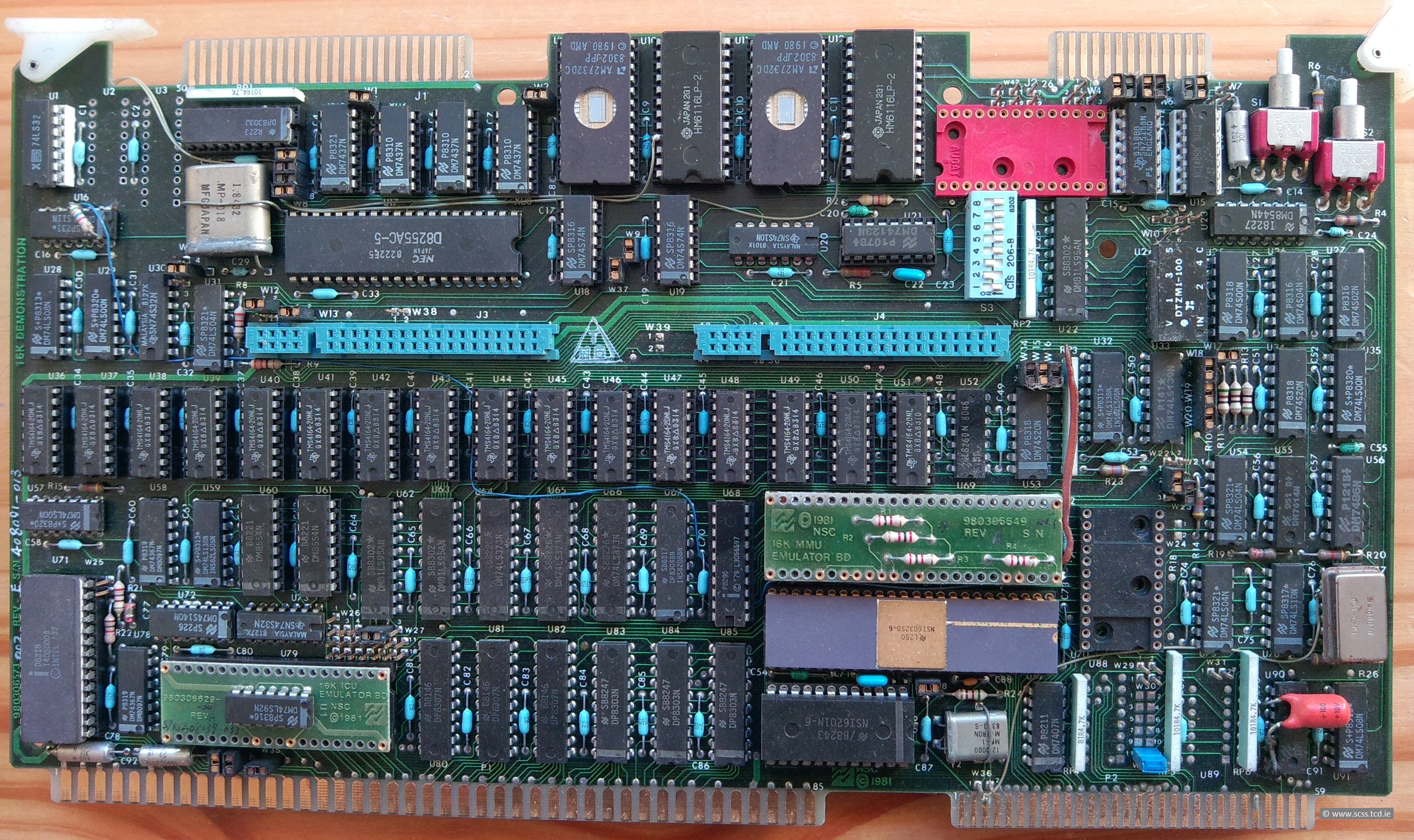
16K DEMONSTRATION (DB16000)
Wow - this board must be one of the very first boards using an NS16000 chip set. The date on the board is 1981! At this time all the parts of NS16000 were in its infancy (buggy) or even not taped out (ready for production). Thanks to The John Gabriel Byrne Computer Science Collection for saving this rare item!
The documentation of the collection says that this board is the DB16000. DB means Demonstrator Board. Unusual the name is not found on the board like it is for the DB32000.

Fig. 1. The 16K DEMONSTRATION board from National Semiconductor
An excellent high resolution version of the photo in Figure 1 is available here. The board used the Multibus standard for an easy integration in existing equipment. 128 kBytes of DRAM memory (U36 - U51) and 4 sockets for EPROMs (AM2732) and/or SRAMs (HM6116LP-2) were provided. It is possible that the blue connectors could be used for memory expanding. I hope that the board is stored in a dark environment to protect the content of the EPROMs because there is no UV filter on top of them ...
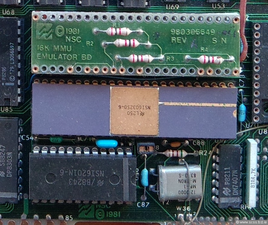
Fig. 2. The CPU "cluster" of the 16K DEMONSTRATION board
The CPU cluster contains only the NS16032 CPU and the NS16201 TCU. The NS16081 MMU is replaced by an emulator board with 4 resistors. Later such an emulator board was not required if the MMU was missing. The NS16201 TCU used a plastic package. This is unusual because the TCU became hot in operation. Maybe the first versions were not so power hungry. It is possible that the design was changed later to support higher speed and more load. But this improvements come always with increased power consumption. It is interesting to note that both devices are not marked as engineering samples.
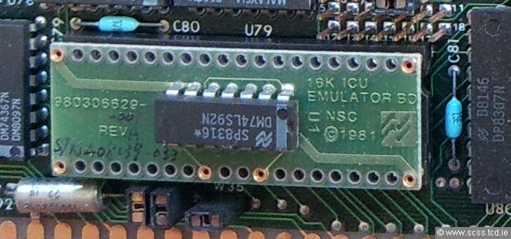
Fig. 3. The "ICU" of the 16K DEMONSTRATION board
At that time even the simple interrupt controller NS16202 ICU was not available. But a DM74LS92, which is a TTL device containing a divide by 12 counter, could do the job. Ok, joke - the ICU is not this simple.
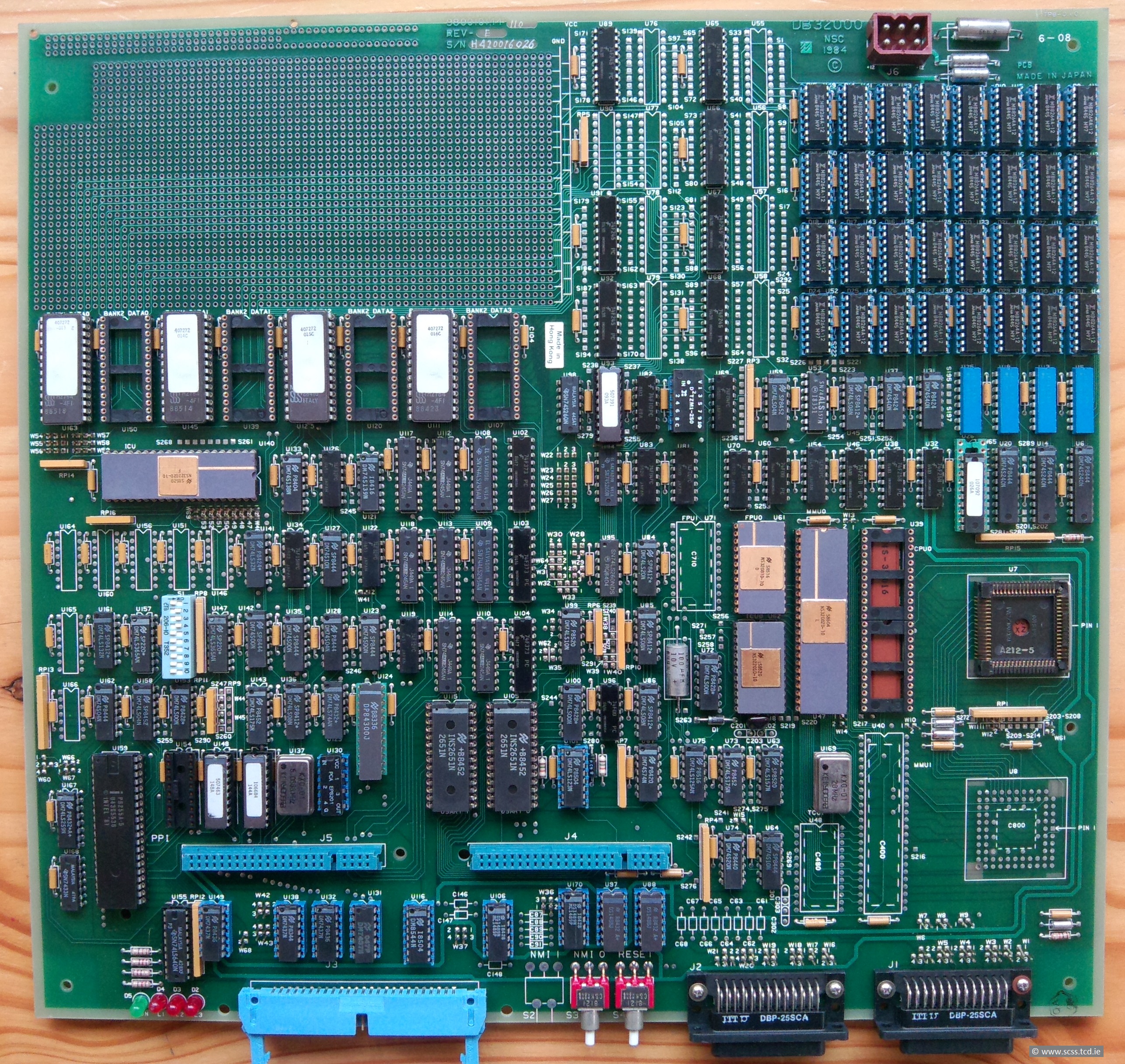
DB32000
The DB32000 is an impressive board simply for its size. Its only purpose was the evaluation of the Series 32000 family. All parts of the first generation could be used. For some unknown reason the board in Figure 4 has no CPU in its sockets, neither the NS32016 CPU nor the NS32032 CPU. It looks like the board is prepared to hold a second NS32032 CPU with its own MMU. But no information can be found about this option in the data books describing the DB32000. Maybe this board was prepared to use two of the mythical NS32132 CPUs.
The board has no standard bus connectors but features a large wire-wrap area for user circuitry. Up to 1 Mbyte of DRAM memory is available. Eight 28-pin sockets for ROM/EPROM allow 256 kbytes of permanent memory. The DB32000 can operate stand-alone with no assistance from a host computer system. Optionally, the board can be operated in conjunction with a host, taking advantage of more powerful software development tools.
The collection owns three DB32000 boards. Two of them have the NS32032 CPU installed. They saved in addition a lot of printed documentation and some software on reel-to-reel tapes. I hope that someone will read the tapes one day and present the content in the web.
Fig. 4. The DB32000 board of National Semiconductor
The two black 25-pin connectors were used for serial RS232 communication links. It was possible to connect the board to a terminal and a host simultaneously. Please note that the board shown was manufactured in Japan.
The photo in Figure 4 is already very good. But if you want even more resolution look here. More photos can be found in a document at the SCSS Treasures Catalog. Use the link TCD-SCSS-T.20141120.007.pdf to open the document.
DB32016 (DB16000A)
In November 2017 I got a parcel from Finland. The main attraction was a DB32016 board. Beside this it contained two Evaluation Kits and a lot of documents. All together was laying around at an university for a very long time.
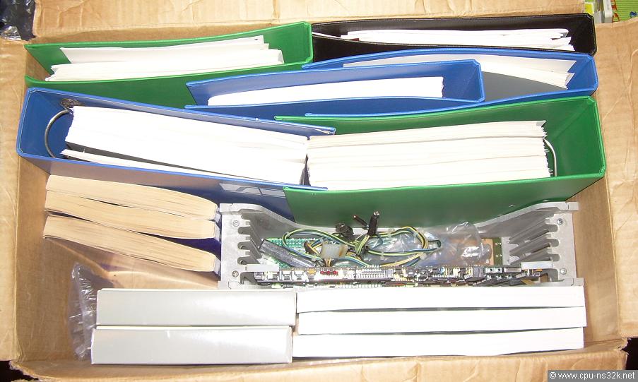
Fig. 5. The parcel from Finland was quite heavy and full of stuff.
The DB32016 board was first named DB16000A. It is very similar to the DB16000. One difference is the use of PALs.
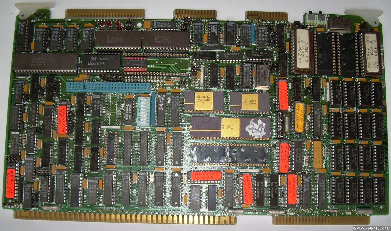
Fig. 6. The DB32016 board from National Semiconductor. 128 kBytes of DRAM are located at the right edge
The system uses 5 V and +/-12 V for RS232. Current consumption of my board is 3.7 A at 5 V.
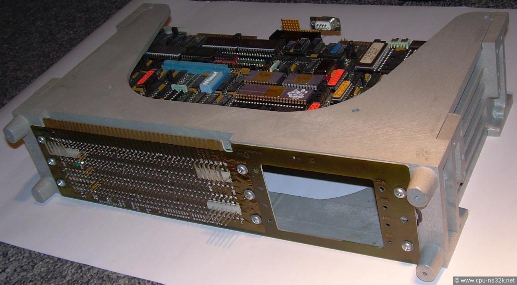
Fig. 7. The cage for the DB32016 board was designed for the Multibus and manufactered by Intel. It is very robust.
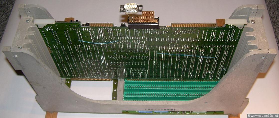
Fig. 8. The backside of the DB32016 board. The cage is ready to hold three more boards.
The great question was: is the board still functional? I was very curious. I modified an old power supply and luckily found an edge card connector in my boxes for the serial interface (see it in Figure 8).
The start was promising. A message appeared on the screen, telling me that the board passes the selftest. But then the message was repeated and the process didn't stop. There was no reaction to any keyboard input. Not the result to open a bottle of champagne...
My hope was that some bits in the EPROMs had flipped over the last 30 years. I exchanged them with some new 27128 devices. But the result was the same. Therefore I have to dig deeper to find the root cause. My candidate now is the CPU. But I will first check what the program is doing.
In-depth Analysis
I started with a simulation of the program on my M32632. I had to add a simple Intel 8251 UART model. In addition I disassembled the code. Now I got a good overview about what was happening during the selftest.
I found the instructions which sent the mentioned message. I also found a signal which is only active during selftest. It is called "DIAG_MODE" and it can be used as a trigger signal for an oscilloscop or logic analyzer. Between "DIAG_MODE" becoming inactive and active again there must be the problem. I decided to use a logic analyzer. The measurement setup is shown in Figure 9.
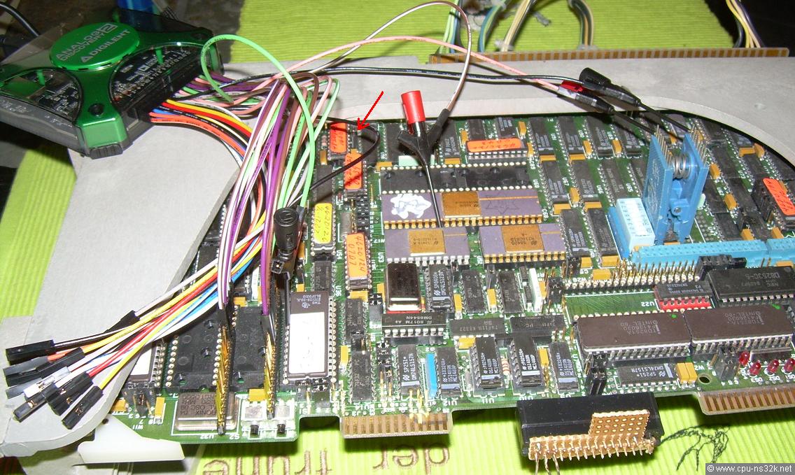
Fig. 9. The measurement setup used an USB logic analyzer with 16 channels from Digilent. The red arrow points to the jumper which caused the loop behavior.
Most of the channels took address signals. It was easy to connect them to the empty EPROM socket. The signal trace in Figure 10 shows the moment when the error happened. Between -25 µs and -15 µs the wait loop at address x'102 is executed. After the loop a CXP (Call External Procedure) instruction should follow. In my opinion this instruction is not executed because the three writes for saving the program counter and the mod register are missing.
For me it was obvious that the CPU must be broken. I replaced the device - and got the same behavior. Uuuh! After some thinking about other possibilities and studying the schematics and the documentation I identified a wrong jumper. There are a lot of jumpers on the board and this one selects the 2732 EPROM. If 27128 are used the jumper has to be removed...
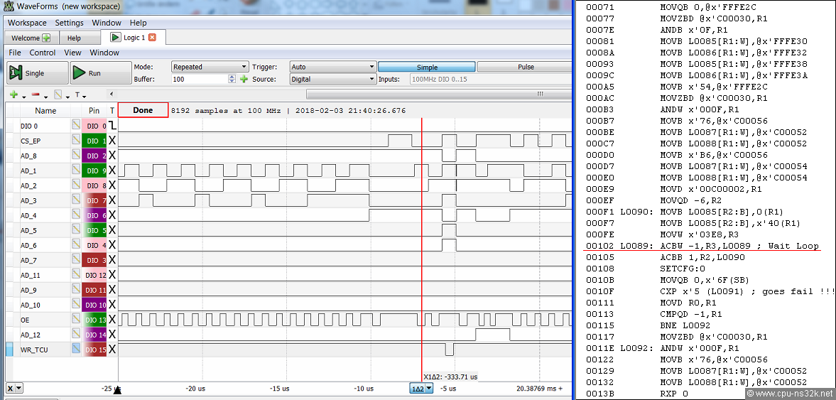
Fig. 10. The signal trace and the program code at the moment when the error occured.
Once again the start was promising. I got the desired TDS message together with the prompt for input. Success! A first dump showed some memory locations. But the disappointment quickly follows. The command "in" to fill the buffer of the editor was answered by the system with a "?". This is the sign for an input error!
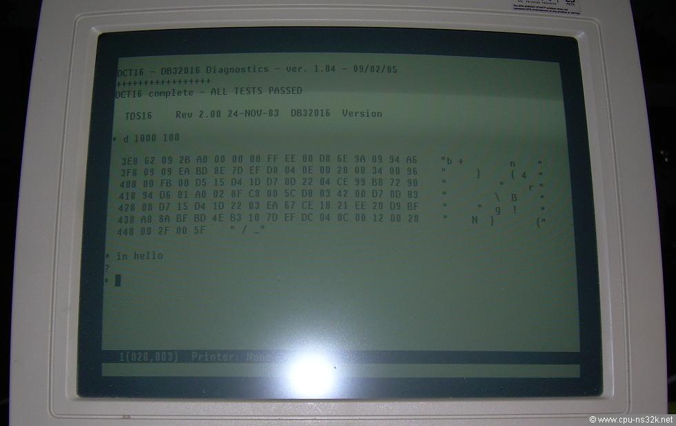
Fig. 11. A screen shot after power up shows one successful command and one failing command.
A look at the command table of TDS showed that the "in" command is not contained in the table. Some other commands are also missing, for example the assembler. This is definitly different from what the documentation says. Therefore the board is useless in the moment.
I have no idea what is going wrong with this version of TDS. Hopefully there are other versions available somewhere.
Thanks to Gilbert!
At the moment I know only one person who has a running system using TDS. It is Gilbert who owns a DB32000. I described him my problem and he sent me a logfile of the communication between his system and the terminal. I saw immediately the cause of my problem: TDS needs after power up an initialization command. Obviously I have not read the manual carefully enough - a bad attitude.
The next screen shot in Figure 12 shows a successful command sequence. The DB32016 is connected to my NS32532 based TITAN3 which I use as the host. The green text on black background is the output of the DB32016. It shows the result of a floating point test program. Please note the unusual display of FP numbers.
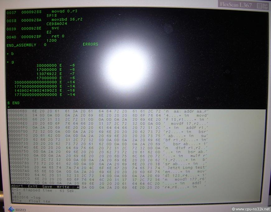
Fig. 12. At the end DB32016 is doing what the user wants. That's the purpose of all computers.
TDS offers read and write commands for using a tape drive as a backup memory. I think it is a better idea to use an SD card for this purpose. It should be no big deal - just an interface to the Intel 8255 PIO and a voltage regulator. The software will be put in two EPROMs which use the free sockets. Then DB32016 is well prepared for being presented at vintage computer exhibitions.
I'm now very happy with the board. Since nearly 20 years I was not able to run programs on an NS32016 CPU. And it is my first running vintage computer.
Is it a surprise that I will be looking for a second DB32016?
ICM-3216
National Semiconductor designed the ICM-3216 for OEMs who needed an embedded computer for their products. Obviously they were very proud of this product as the following advertisment shows.
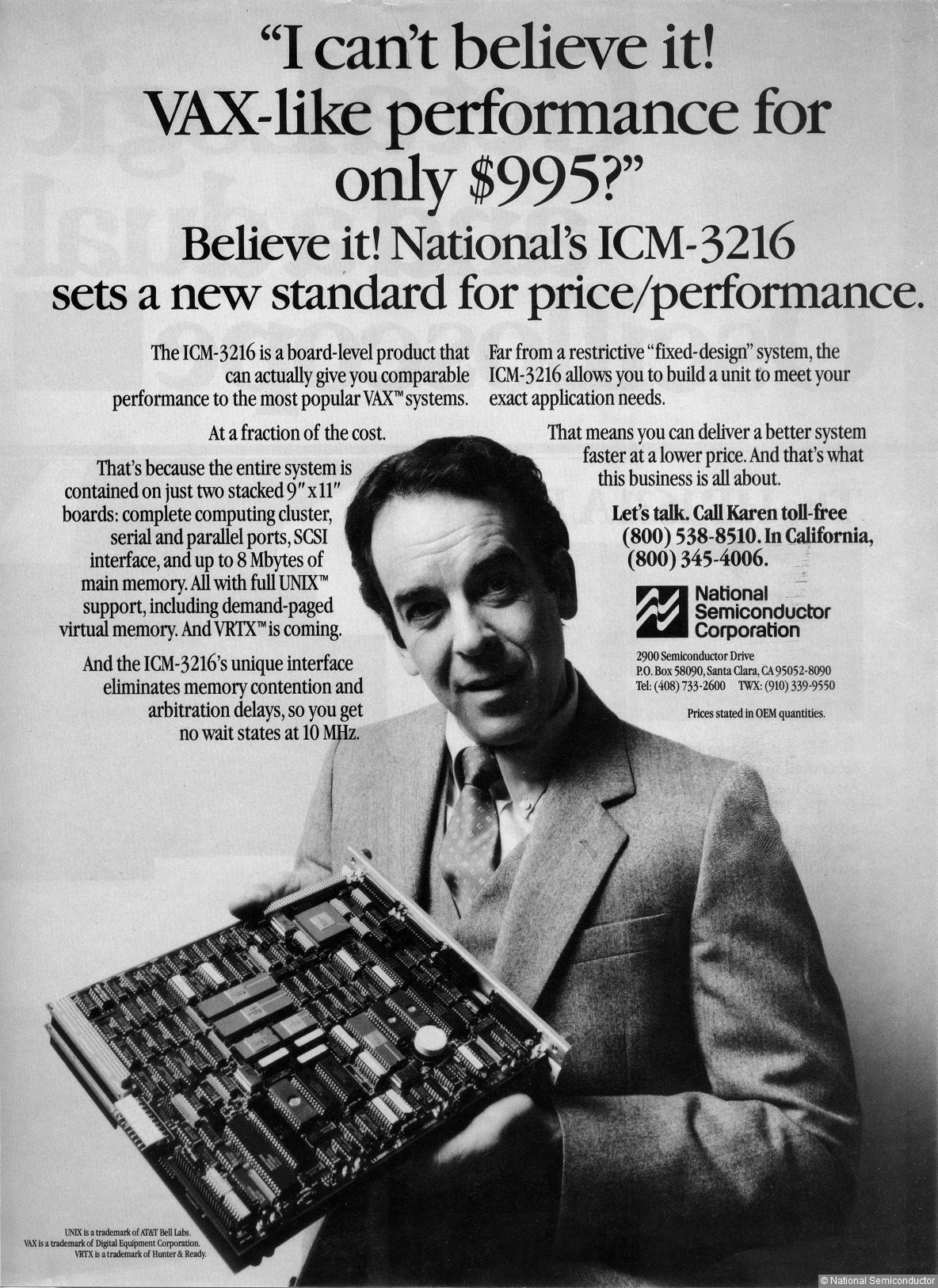
Fig. 13. Every product is simply the best...
The "Integrated Computer Module" ICM-3216 is a complete computer system contained on two 11.02 in. (300 mm) x 9.18 in. (233 mm) printed circuit boards. One board contains the CPU cluster, PROM sockets, four serial interfaces, address mapping logic, SCSI interface, parallel port, memory interface and the MiniBus interface, see Figure 14. The other board contains the DRAM memory. The CPU cluster is based on the NS32016 CPU running at 10 MHz and used all support chips. A third board is available which adds 8 serial ports to the system.
The SCSI interface was used to attach hard disk drives and tape units. It used an LSI SCSI device (below the label "UNIVERSITY OF NEW BRUNSWICK" in Figure 14) and a Z80B microprocessor. This solution took away the details of the data transfer from the NS32016.
The photos are taken by Steven who owns a complete ICM-3216 system. Thank you very much for the great photos!
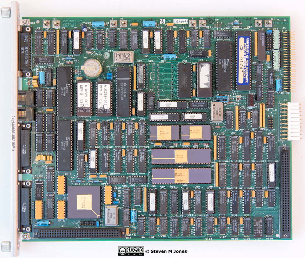
Fig. 14. The ICM-3216 CPU board. The photo is available in higher resolution here.
The ICM-3216 system didn't use the traditional backplane boards to connect multiple boards together. It used instead of it female connectors on the component side and in the same place male connectors on the solder side. The boards were simply pressed on each other. Power was also delivered this way with matching connectors. 4 pairs of power and ground are placed at the upper edge in Figure 14.
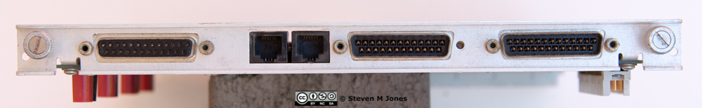
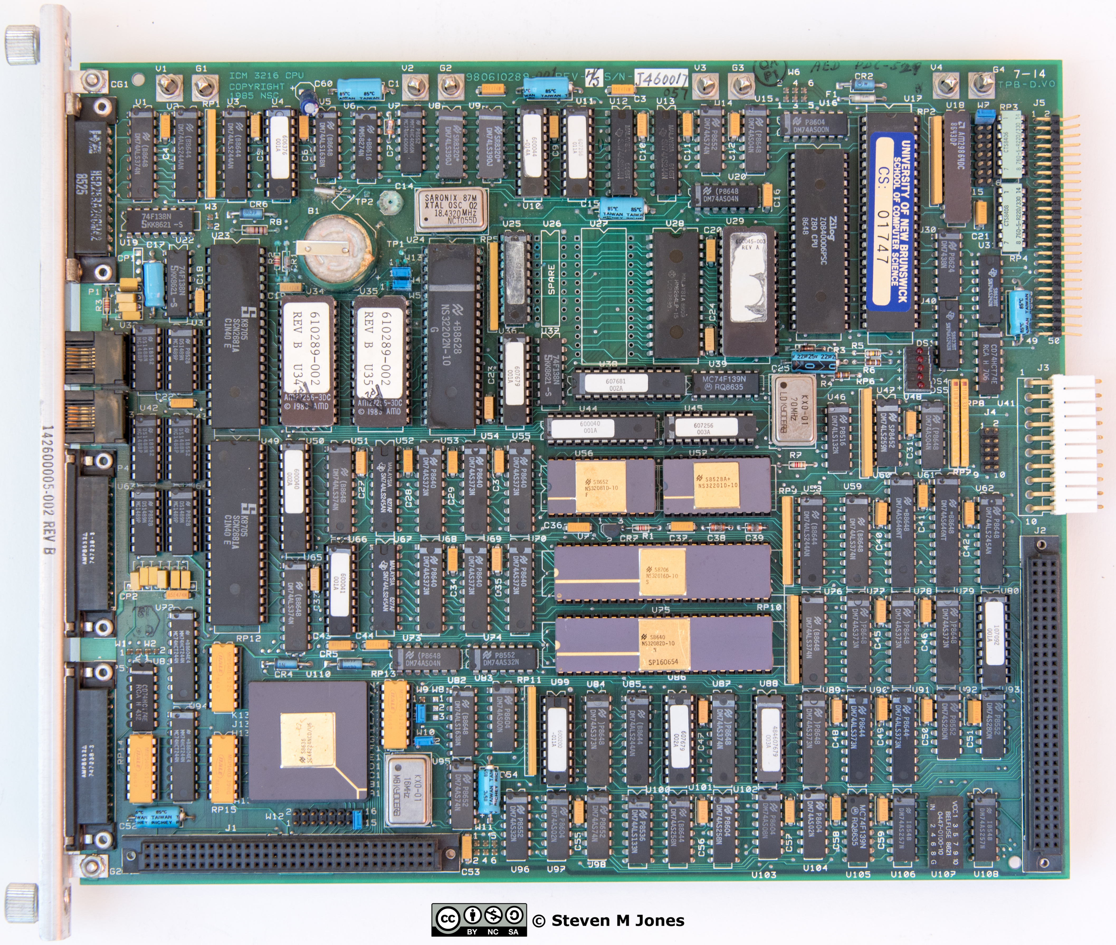
Fig. 15. The front side of the ICM-3216 CPU board. Please note that there is no reset button...
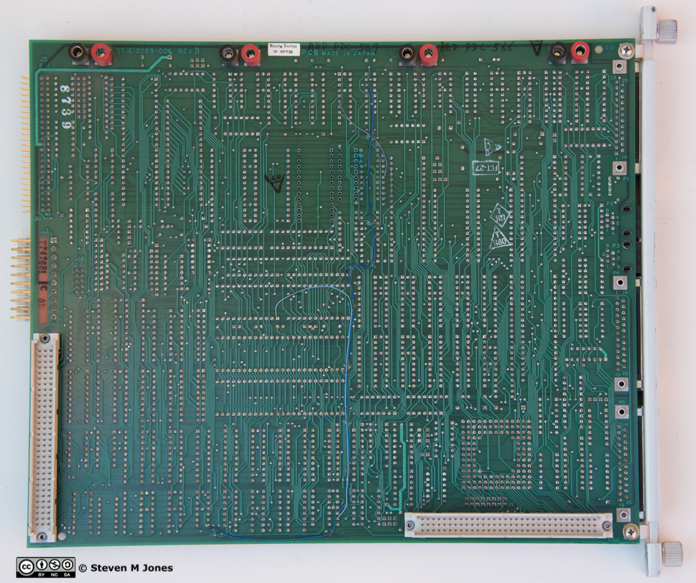
Fig. 16. The backside of the ICM-3216 CPU board shows the male connectors.
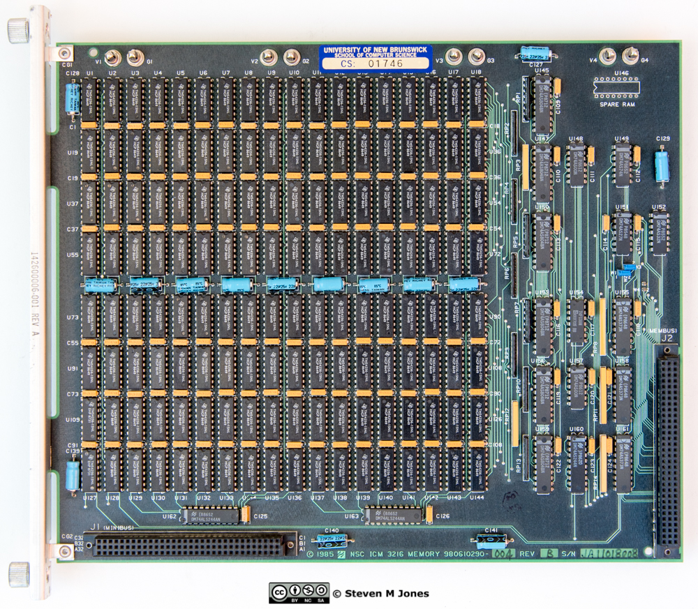
Fig. 17. The ICM-3216 memory board. The photo is available in higher resolution here.
The memory board holds 144 256-Kbit DRAMs for 4 MBytes of memory with parity protection.
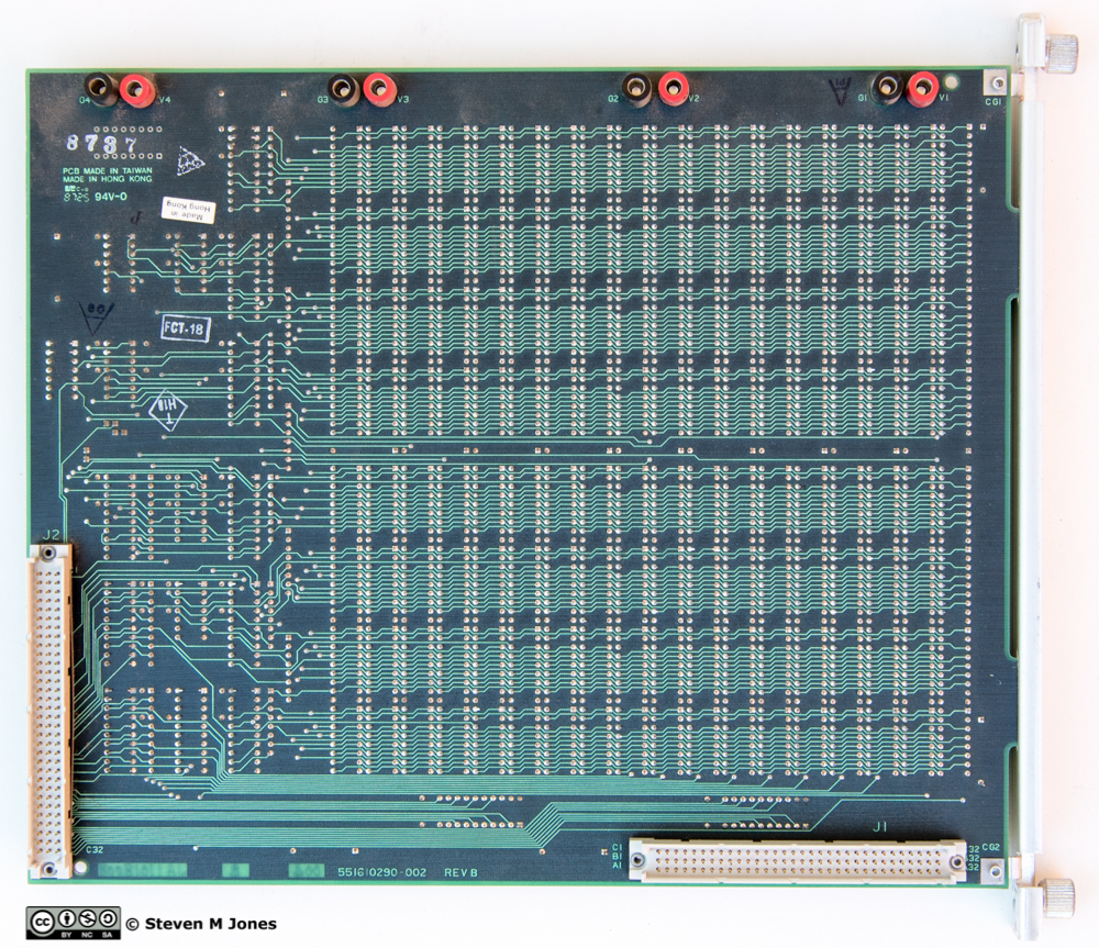
Fig. 18. The backside of the ICM-3216 memory board.
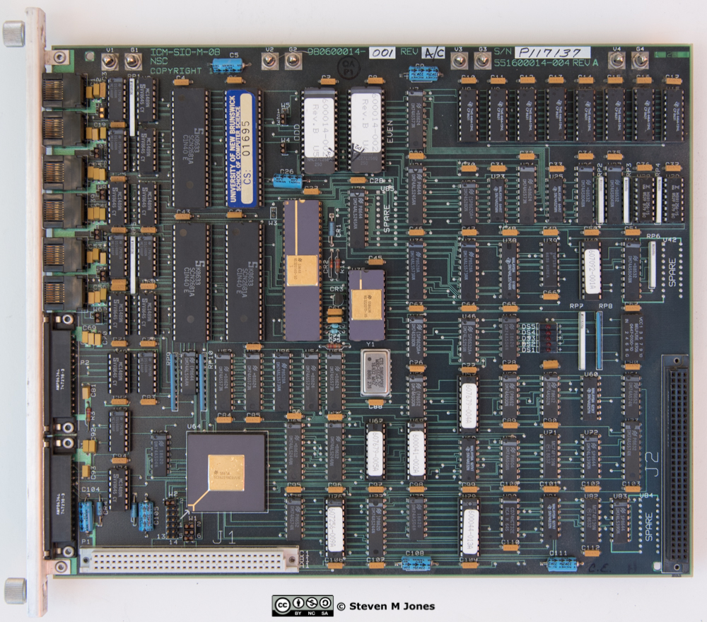
Fig. 19. The ICM-3216 serial board. The photo is available in higher resolution here.
The serial board uses an own NS32016 CPU running at 9.216 MHz. The quartz oscillator of 18.432 MHz is reused to generate the standard baud rates. Memory is 64 kBytes of EPROM and 256 kBytes of DRAM.
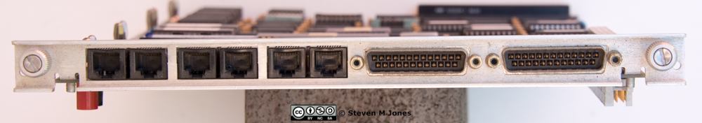
Fig. 20. The front side of the ICM-3216 serial board. I have never seen a terminal with a connector like the left six ports.
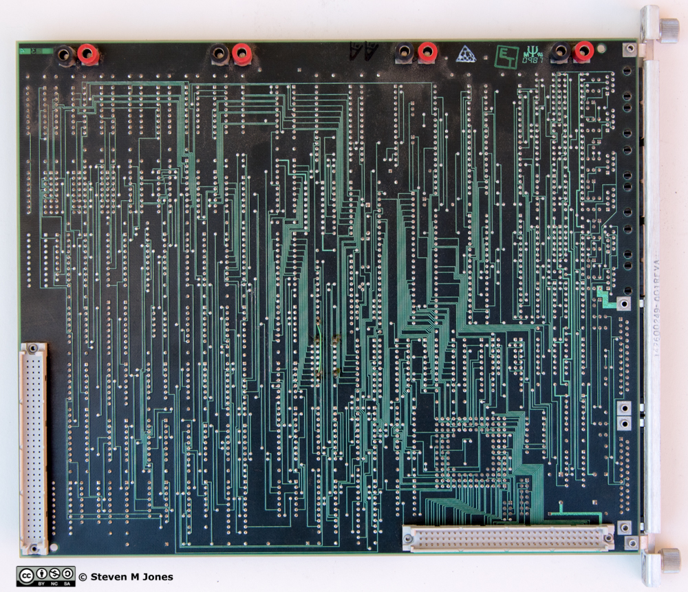
Fig. 21. The backside of the ICM-3216 serial board. Please note that it has no connection to the memory bus because the left connector has no pins.
There are a number of documents available describing the ICM3216 and the MiniBus.
ICM-3216 Preliminary Datasheet
ICM-3216 CPU Board Specification
ICM-3216 Memory Board Specification
ICM-3216 ROM Monitor User's Guide
MiniBus Interface Chip Specification
The University of Toronto distributed a 4.2BSD port for the ICM3216. This was announced in 1987 in a usenet post, see it at https://groups.google.com/g/mod.newprod/c/10BSxSNszdw .
I suppose that all the bits of this software are now in another universe...
Thanks to Steven for the finding of this post.
VME532
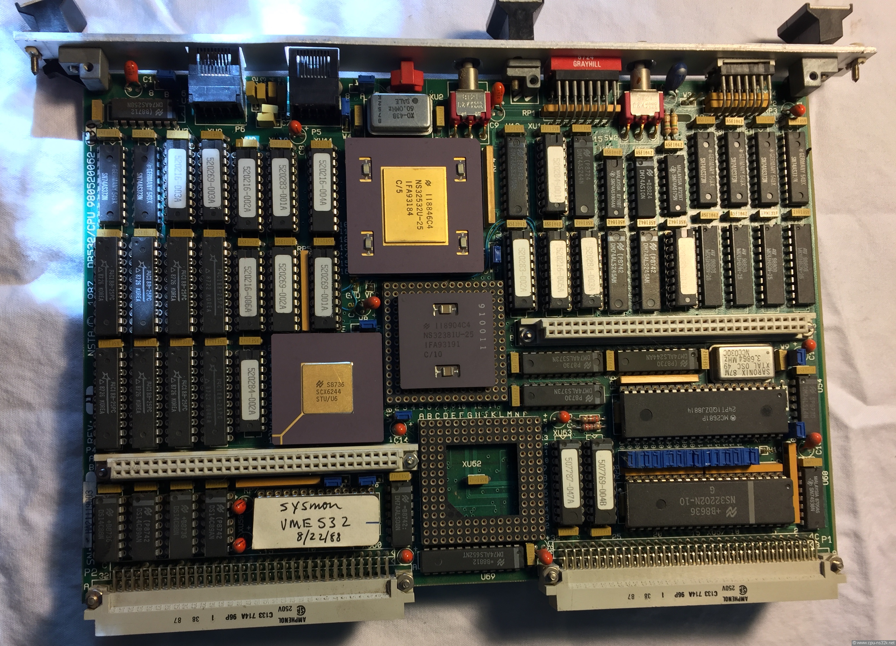
The VME532 was the most powerful board level product of Series 32000. It is based on the NS32532 CPU. The VME532 consists of two boards which are closely connected by a local bus: a CPU board and a memory board. The boards are made according to the VME bus standard and can be mounted in a VME rack. The size of the pcbs is 233 x 160 mm. Figure 22 shows the frontside of the VME532 pair.
Fig. 22. The front side of VME532. The selector for the CPU ID is placed on the memory board.
I got the photos from the only person I know who owns a VME532. It is astonishing for me how rare these boards are. Maybe an explanation is that the owner aren't willing to sell this nice board at ebay...
The VME532 CPU board in Figure 23 shows the NS32381 FPU sitting in a larger socket. The board has the option to use the NS32580 FPC instead of the NS32381. For further information see the application brief AB-40. Using the FPC requires also the use of the Weitek WTL3164 FPDP for which the now empty 144-pin socket XU62 is provided.
The owner of the board has long tried to get the NS32580/WTL3164 pair. But he was not successful. It seems that this parts are even rarer...

Fig. 23. The CPU board of VME532. This photo is available in higher resolution here: VME532 CPU.
For high performance the CPU board has a 64 kBytes cache. The data memory of the cache is made of 8 fast SRAMs from Performance Semiconductor. The SRAM device P4C188-25PC is organized as 16k x 4 bits and has an access time of 25 ns. They are located at the left edge. The tag memory of the cache is made of four special SRAMs from SGS-Thomson. The tag memory chip MK41H80N-25 contains a 4k x 4 bits memory array and a 4-bit comparator. 12 address bits and one valid bit are used for the tag. The result is a 256 MBytes cachable address space. The tag memories are located at the right edge. Both types of memory use a 22-pin DIP package.
The VME532 was designed for multiprocessor systems. Up to 16 of these boards could be used in one system. A thumbwheel switch enables user to assign unique CPU identification numbers, ranging from 0 to 15. The local memory could be accessed by other VME masters including other CPUs.
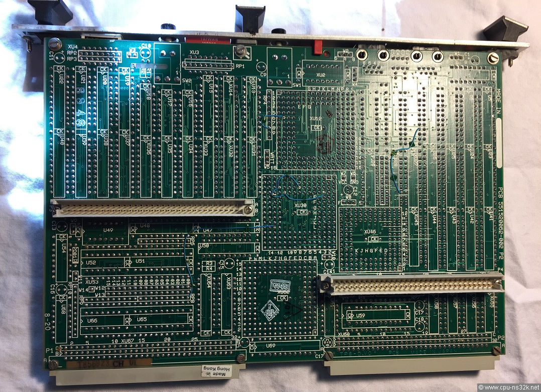
Fig. 24. The back side of the VME532 CPU board. Some wire fixes were necessary.
The backside of the CPU board reveals an interesting detail: some smaller ICs are placed below the bigger ones. For example the device U59 is placed below the 512-kbit EPROM XU60. The EPROM is the device with the label "SYSMON VME532 8/22/88" on it. Two ICs could be placed below each 40-pin DIL device which are the NS32202 ICU and the MC2681 UART.
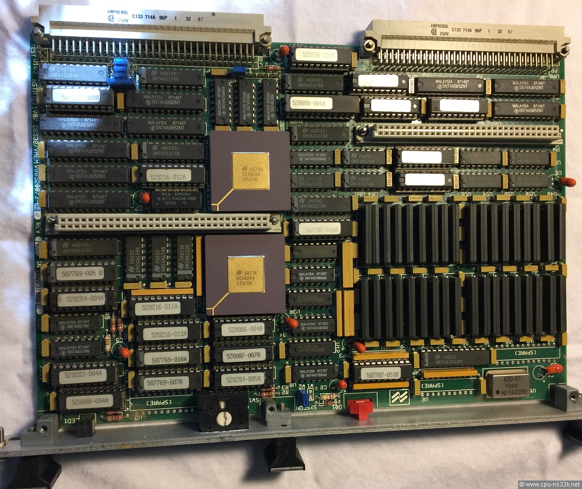
Fig. 25. The memory board of VME532. This photo is available in higher resolution here: VME532 Memory.
The memory board in Figure 25 contains 4 MBytes of parity protected DRAM. 36 1-Mbit devices in ZIP package are used. The DRAMs are soldered to the board. Therefore an easy upgrade to 16 MBytes is not possible although the 1-Mbit and 4-Mbit DRAMs are pin-compatible.
The 1988 data book mentions a 12 Mbyte Local Memory Expansion. This is an additional board (see it in Figure 29) which is mounted between the CPU board and the memory board.
The devices in 124-pin PGA packages with the marking SCX6244 are custom chips. The VME532 development team designed them to implement the DRAM controller and the delayed write buffer. The biggest available CMOS gate array at National Semiconductor of this time providing 2800 gates was used. The design was done manually because of lack of synthesis tools. Nevertheless the custom chip was fully functional at the first shot. A datasheet of SCX6244 can still be found in the internet.
In my view the memory board contains the interface to the VME bus. Quite a lot of SN74AS652 bus transceivers and SN74AS374 register chips are placed near the VME bus connectors at the edge of the memory board.
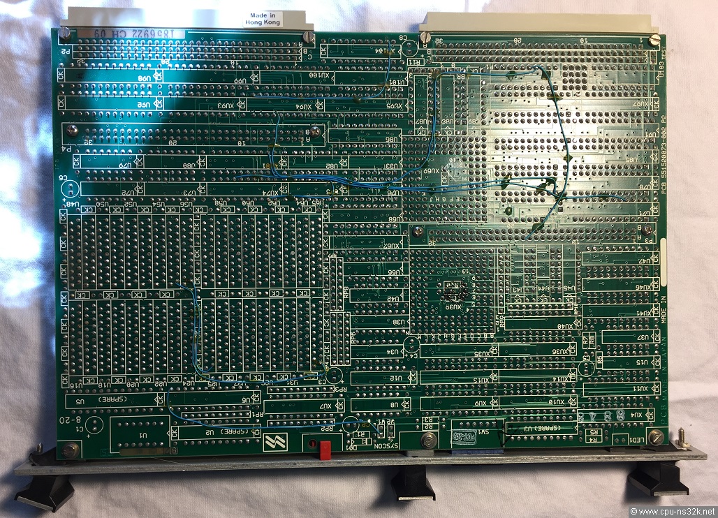
Fig. 26. The back side of the VME532 memory board. Again some wire fixes were done.
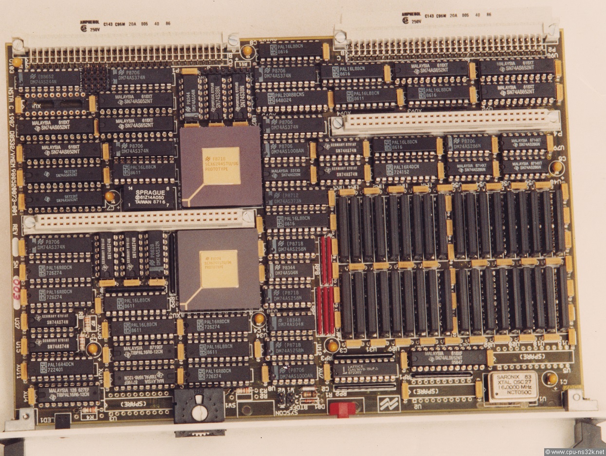
Fig. 27. Another VME532 memory board.
The VME532 memory board in Figure 27 is a noteable one. According to the serial number "3" at the left edge it must be one of the very first boards. Another hint is the marking "PROTOTYPE" on the gate arrays. Very unusual is that no labels are placed on the PALs. How they are identified? A lot of bipolar PALs from MMI and Texas Instruments were used. One electrically erasable PAL from Lattice was already used too. In the photo the GAL16V8 can be found in the middle of the lower edge. In 1987 GALs were very new.
My VME532
In September 2023 George G. sent me an email. He asked me whether I'm interested in getting a VME532. Of course I said yes! The nice thing about his system is that it has the 12 MByte memory expansion for a total of 16 MBytes of main memory.
In October the parcel arrived. Surprisingly the CPU was not in its socket. It looks like it fell off during the journey. Therefore I had doubt that the system is still functional. To test it I needed a VME backplane. But these stuff is expensive even at ebay. I don't wanted to buy one until I'm sure that the VME532 is okay. So it took another year until a friend came by with his backplane.
And the worst case scenario became true. After switching on power the SYSFAIL LED shines. And it didn't go off. It turned out that the CPU made no access of the boot EPROM. A very strange behavior which normally tells you that the CPU is broken. But I was sure that this CPU was okay because I took it out of a running system. What to do?
Some days later I took the CPU out because I wanted to measure the HOLD signal. This might be a reason for the CPU to not access the EPROM. The CPU came out of its socket relativly easy. This was not normal for a 175 pin PGA. Could it be that not every pin was connected? I put the CPU in again with strong force. I don't like this. My designs uses ZIF sockets. But the action was successful - the VME532 booted!
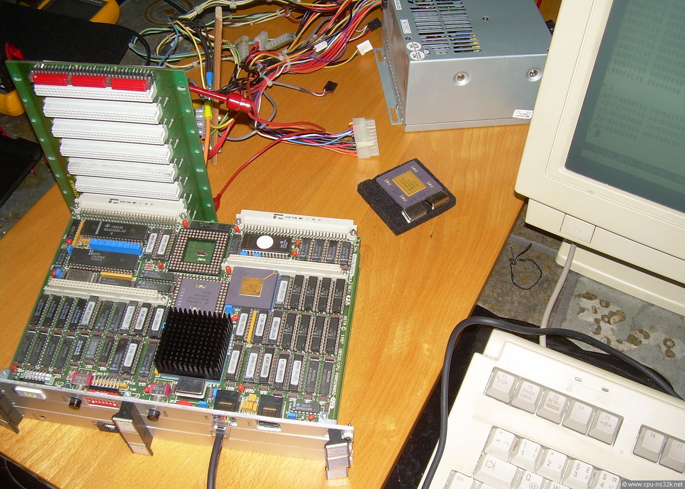
Fig. 28. My VME532 during the first successful tests. You can see some output on the screen on the right side.
The three boards system is very power hungry. I used first my old linear power supply which can deliver 10A at 5V. But it was already at its limit. So I used finally an old PC power supply. The CPU got a heatsink to improve its lifetime.
Unfortunately the system came without any documentation. The system monitor SYSMON has a simple help page. There is a download command over the RS232 port. But it doesn't tell the format. So I read out the 27C512 EPROM content and analyzed the code with a disassembler. The download format is simple and soon after I was able to run some small test programs. Further information was gained about the baud rate selection. This is done by the DIP switches 1 to 4 on the front panel. The VME532 came with 9600 Baud which is uncomfortable slow. I could change this to 38400 Baud.
It became clear that I can run my TITAN3 operating system on the VME532. Of course not with any mass storage at the moment. But it supports a RAM disk and therefore also VME532 can run all of my own programs. Some changes are necessary due to the used UART and the ICU NS32202. At least it took only one day of hard work to get the software running. The seven segment LED on the front panel was very helpful during debugging.
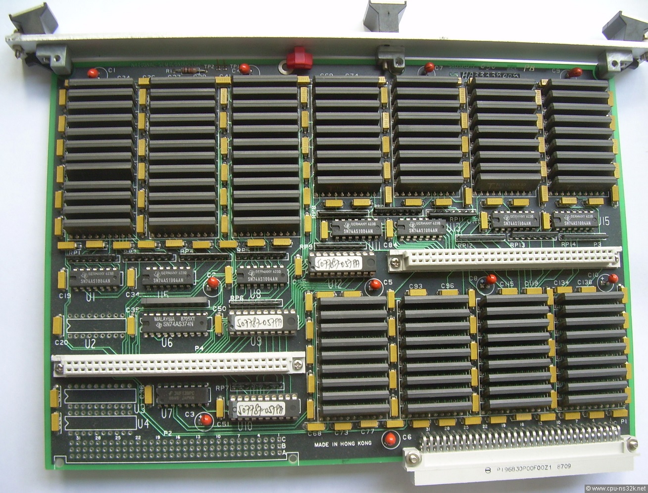
Fig. 29. The 12 MByte memory expansion board is made of 108 1 Mbit memory chips, some fast TTL buffers and some PALs.
It was interesting to compare the performance of VME532 and TITAN3. Both systems share some charachteristics: they use a 25 MHz CPU and have 16 MBytes of main memory. TITAN3 has a very fast DRAM access. The DRAM data path of VME532 seems to be complex and slow. To compensate this disadvantage it has a level 2 cache of 64 kBytes. The test contains a compilation of a JPEG decoder written in pascal, an assembler run of the JPEG decoder, a run of the JPEG decoder which generates a true color image and an md5 run which calculates a hash value for the image. This is done to see whether the results for VME532 and TITAN3 are identical. Here are the run time numbers:
| Task | TITAN3 | VME532 | Difference |
|---|---|---|---|
| Pascal Compiler | 1.060 s | 2.039 s | +92.4 % |
| Assembler | 1.467 s | 3.385 s | +130.7 % |
| JPEG decoder | 52.947 s | 79.875 s | +50.9 % |
| md5 check of image | 2.049 s | 2.815 s | +37.4 % |
The results were not as expected. VME532 was much slower than TITAN3. Is the level 2 cache active? To find this out I wrote a small testprogram which reads 5000 integers from memory twice. After the first read the data should be in the cache and the second read should be faster:
| Task | TITAN3 | VME532 | Difference |
|---|---|---|---|
| initial read | 2.006 ms | 3.692 ms | +84.0 % |
| 2. time read | 2.002 ms | 3.681 ms | +83.9 % |
The result for TITAN3 was as expected. It has no level 2 cache. But the VME532 behaves similar: no level 2 cache. To find a reason for this I disassembled again parts of SYSMON because it shows some messages about cache testing at boot time. I learned that the cache content can be fully defined by software. This feature is very useful for testing the cache. Two bits control the cache behavior: one resets the tag ram and the other locks the cache content. This lock bit was set during my tests. Unlocking the cache results in the desired run times, see the following tables:
| Task | TITAN3 | VME532 | Difference |
|---|---|---|---|
| initial read | 2.006 ms | 2.610 ms | +30.1 % |
| 2. time read | 2.002 ms | 2.022 ms | +1.0 % |
The run time for the second read is now the same for both computers. I rerun also the application test. The result shows the importance of the level 2 cache for performance:
| Task | TITAN3 | VME532 | Difference |
|---|---|---|---|
| Pascal Compiler | 1.060 s | 1.133 s | +6.9 % |
| Assembler | 1.467 s | 1.575 s | +7.4 % |
| JPEG decoder | 52.947 s | 53.256 s | +0.6 % |
| md5 check of image | 2.049 s | 2.139 s | +4.4 % |
Fig. 30. My old prommer from 1987 on the left side needs a new host. It can read and program 27C512 EPROMs.
The next step will be to add a peripheral board to the VME bus. It will use an old ACEX FPGA for 5V compatibility and will contain an SDC interface for file storage, an Ethernet port and a real time clock.
What is really exciting about my VME532 is the option to add a Weitek WTL3164 floating point data path. The functionality of the ungetable NS32580 must be realized by another ACEX FPGA...
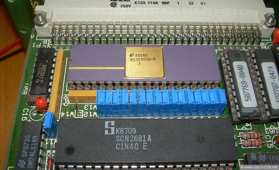
Fig. 31. In my opinion the ceramic version of NS32202 looks much better than the plastic version - I exchanged them 😊
SYS-16/SYS32
Ian is a hero. He saved in Summer 2023 an old computer named SYS-16 from being scrapped!
SYS-16 is an astonishing system. I didn't notice it until Ian asked me about it. I looked in my databooks but I didn't found anything. There is a SYS32 described in the 1984 edition. The 1986 edition does not contain SYS32. National Semiconductor must have stopped selling it sometimes after 1984.
But the photo of the system I got from Ian told me that SYS-16 must be equal to SYS32 - see Figures 31 and 32. The name was changed due to the general name change from NS16000 to Series 32000 in 1984.
Why is SYS-16 astonishing? It is a huge system. It has many features and looks like a minicomputer. It can compete with machines like the VAX11/750 from Digital Equipment. Nothing that National Semiconductor built after it came close to this system.
I'm really curious about the price. SYS-16 was for sure not a cheap computer and in addition the development must have cost a lot of money. But it doesn't seem to be a success in the market. Why? I think there are two technical reasons. First it was a 16-bit machine. In the beginning of the 1980's customers started to ask for true 32-bit machines. True means 32-bit microprocessors which have an external databus of 32 bits. Vendors began quickly designing 32-bit versions of existing 16-bit ones. The NS32032 CPU was the result of National Semiconductor efforts - in my opinion a bad result. It would have been much better if the first 32-bit version was the NS32332 CPU.
But what does this mean for SYS-16? It must be redesigned from the ground-up. This was obviously not done. Because it was too expensive? Most probably yes. The second reason was the lack of a network connection. There is simply no hardware for it. And due to the custom bus it was not possible to use a product from the market - another strategic mistake.
And now after all negative statements let's have a look at a great machine.
Fig. 31. The Series 32000 databook of 1984 describes the system SYS32 which is a renamed SYS-16.
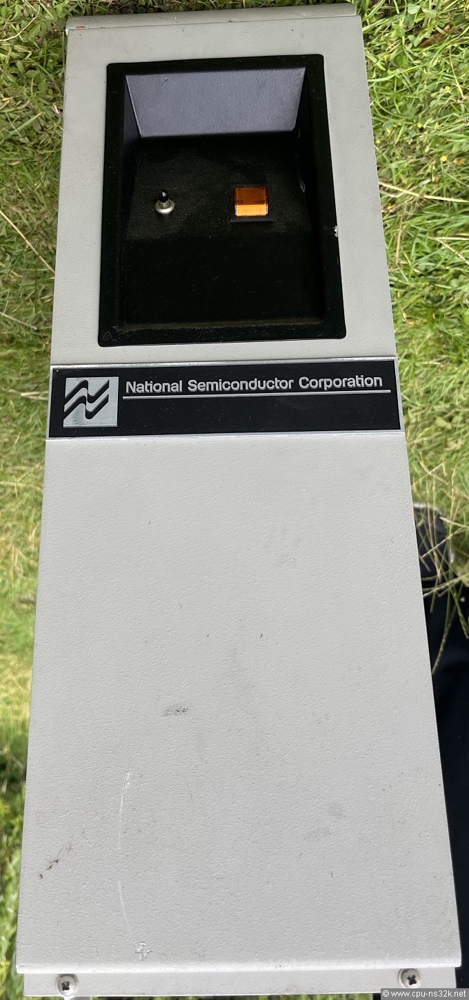
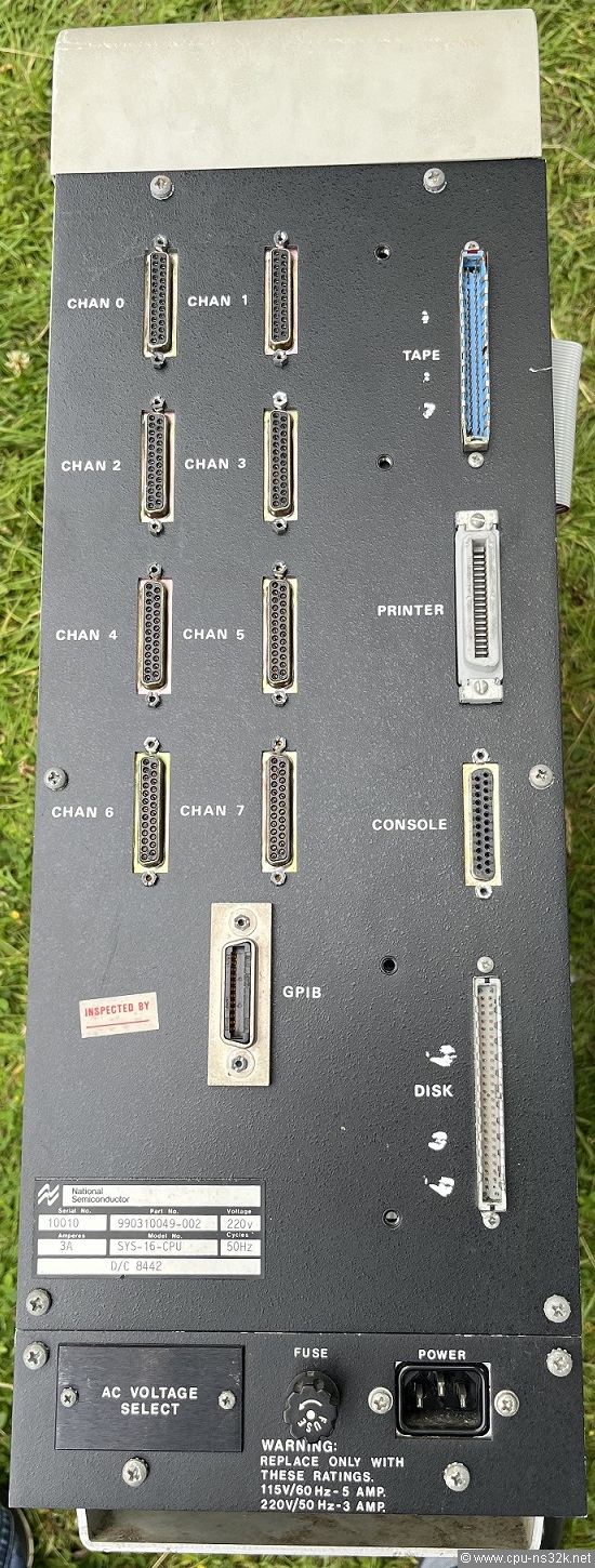
Fig. 32/33. The frontside is not exciting. Maybe the designer was in a hurry. Or there was none. The backside shows that this system was made for Europe.
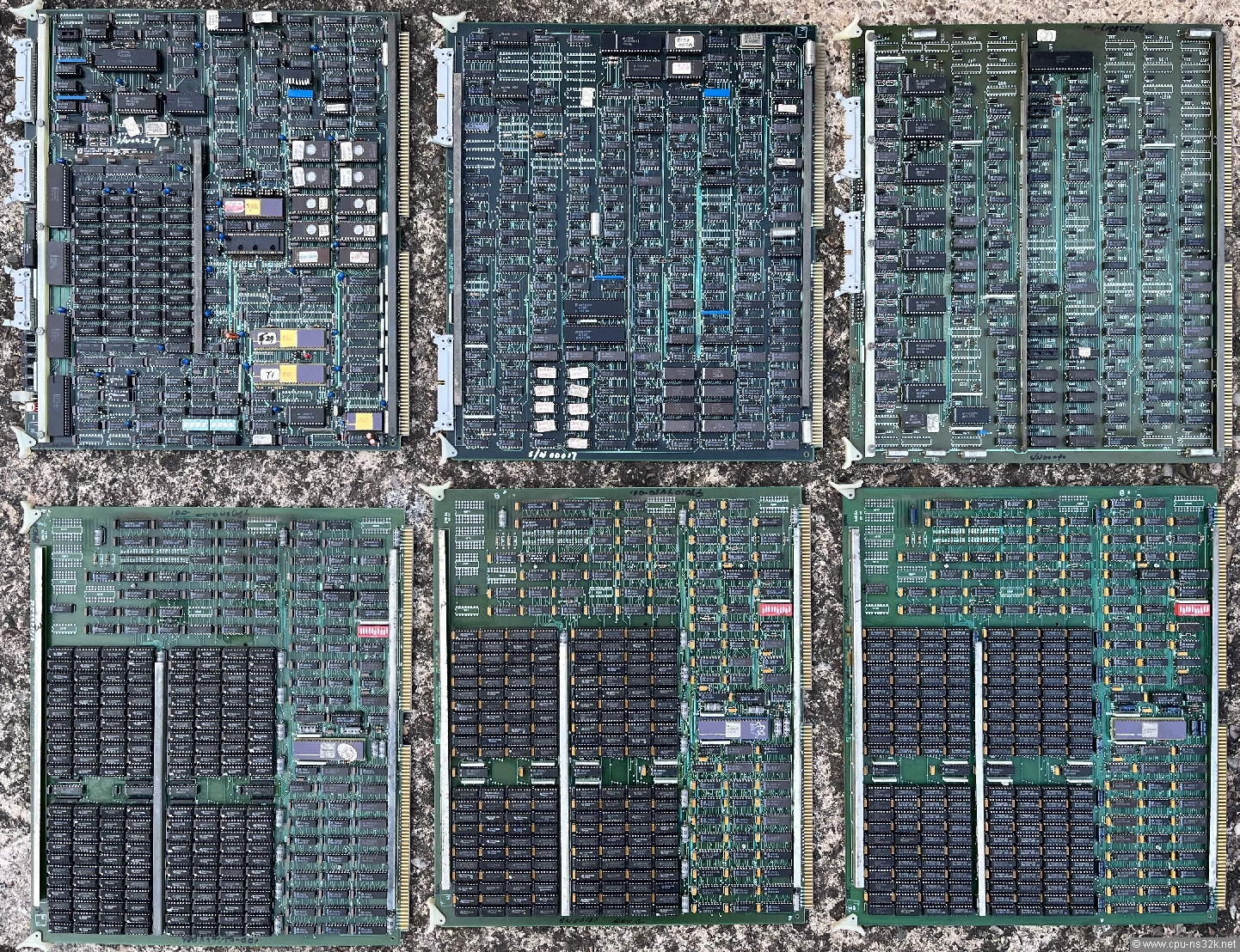
Fig. 34. Together all six boards of a SYS-16 have a memory capacity of 3.25 Mbyte. Board size is around 376 mm by 323 mm.
Figure 34 shows in the top row from left to right the CPU board, the disk and tape controller board and the serial controller board. The serial board has 8 channels. The bottom row shows three memory boards. Each stores 1 Mbyte. SYS-16 were sold with one to three memory boards. It could also been upgraded in the field later. Please note the different settings of the red DIP-switches on the memory boards.
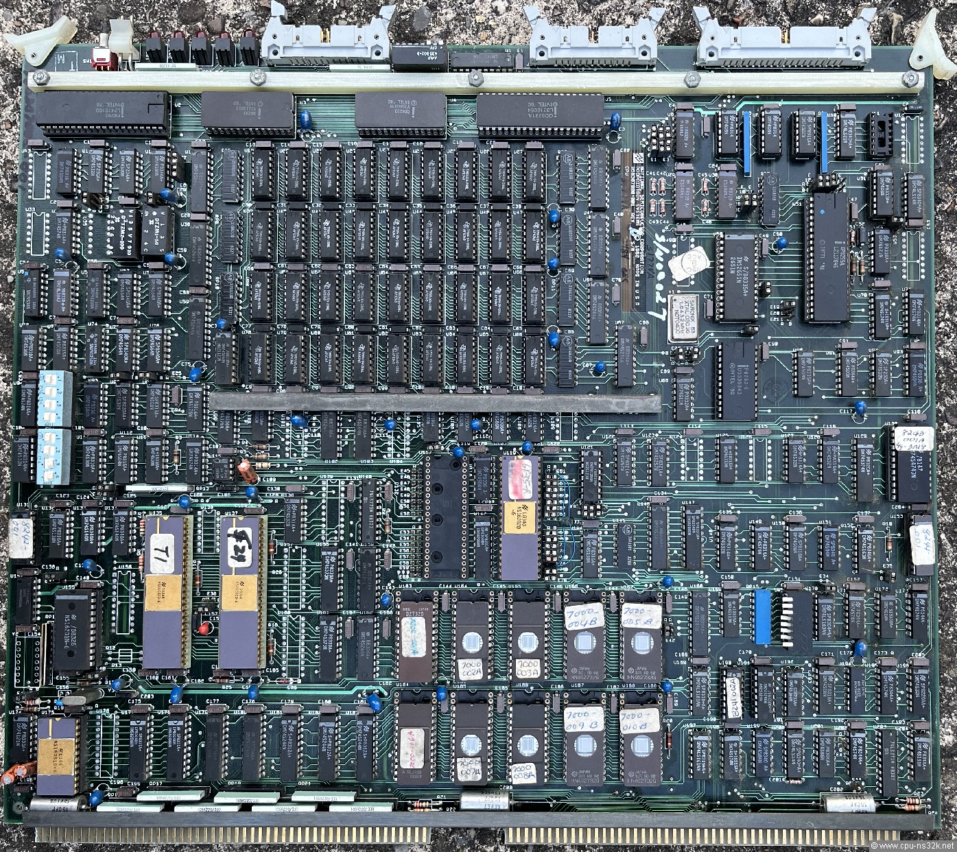
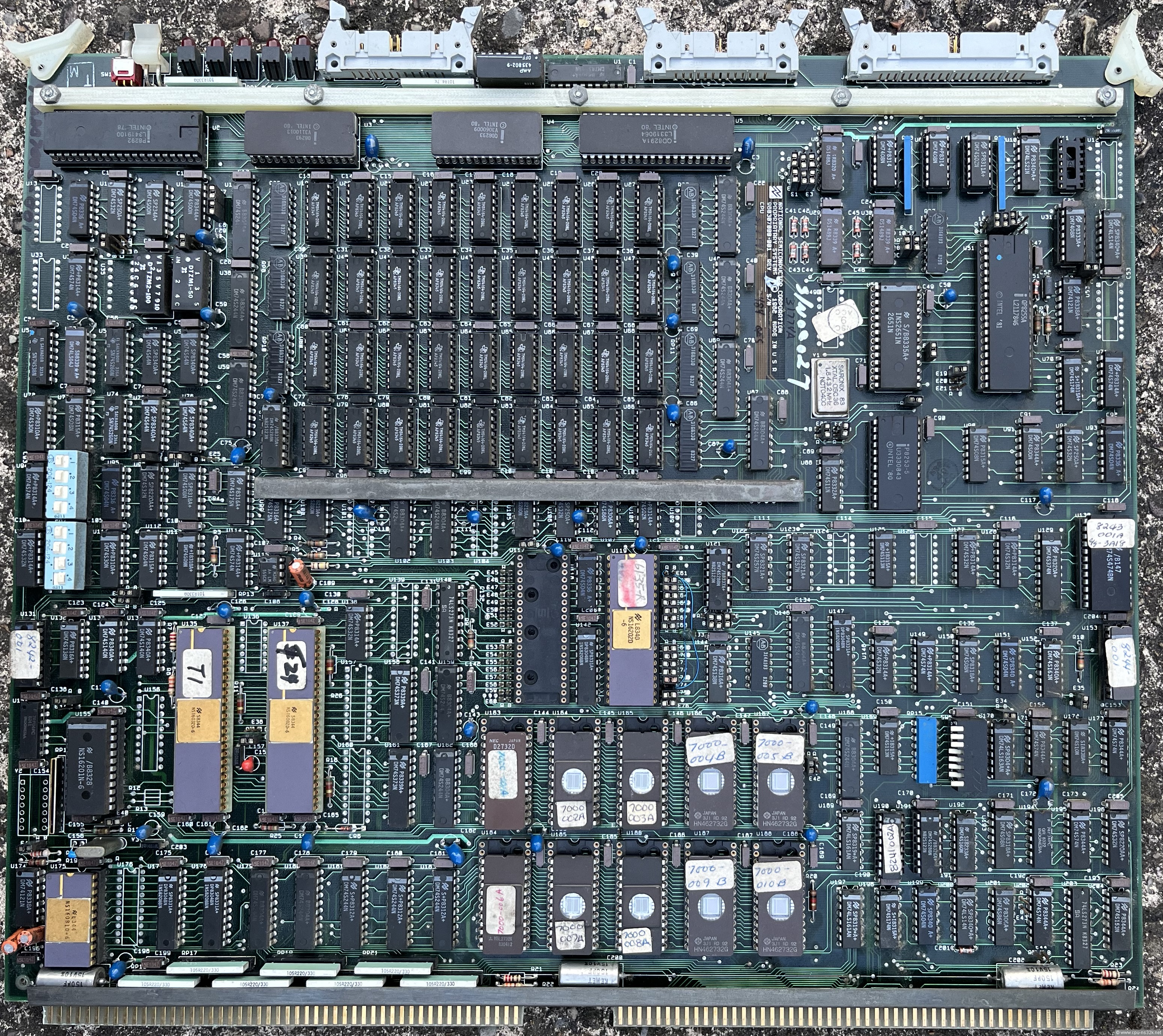
Fig. 35. The CPU board of SYS-16 contains 256 kbytes of parity protected DRAM. The photo is available in high resolution.
There are ten sockets for EPROMs on the CPU board. They can be used for DIP-24 and for DIP-28 devices. This board uses only 2732 EPROMs for a total memory of 40 kbytes.
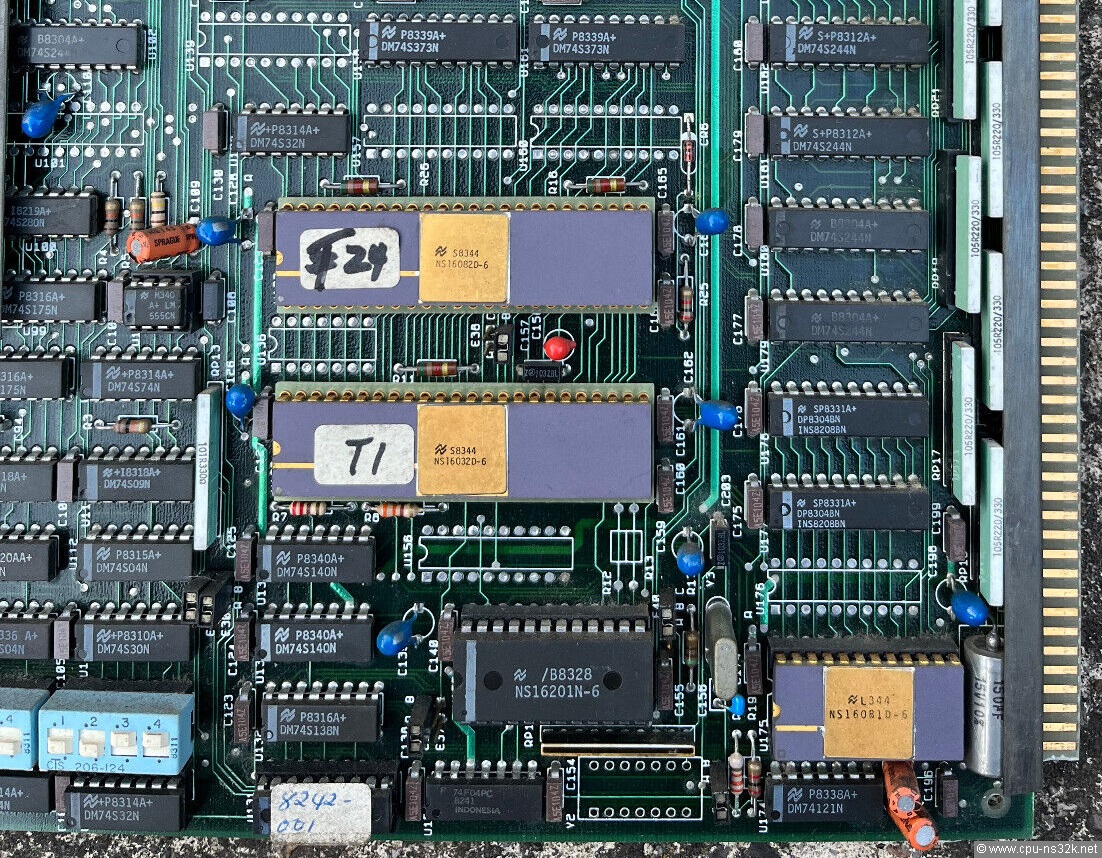
Fig. 36. The CPU cluster is made of very early parts of Series 16000. Due to their bug status the system must have used many workarounds in software and hardware.
I don't know whether SYS-16 ever used 10 MHz devices for the CPU. The system shown here is slow due to the 6 MHz devices. But the whole machine uses TTL devices of the Schottky type which are fast and could potentially support 10 MHz.
In the beginning of his career the NS16201 TCU used a plastic package. Later it was put in a ceramic package because of the high power consumption.
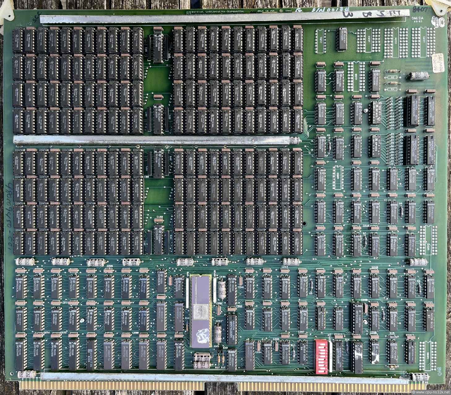
Fig. 37. The memory board of SYS-16 contains 1 Mbyte of SECDED protected DRAM. The photo is available in high resolution.
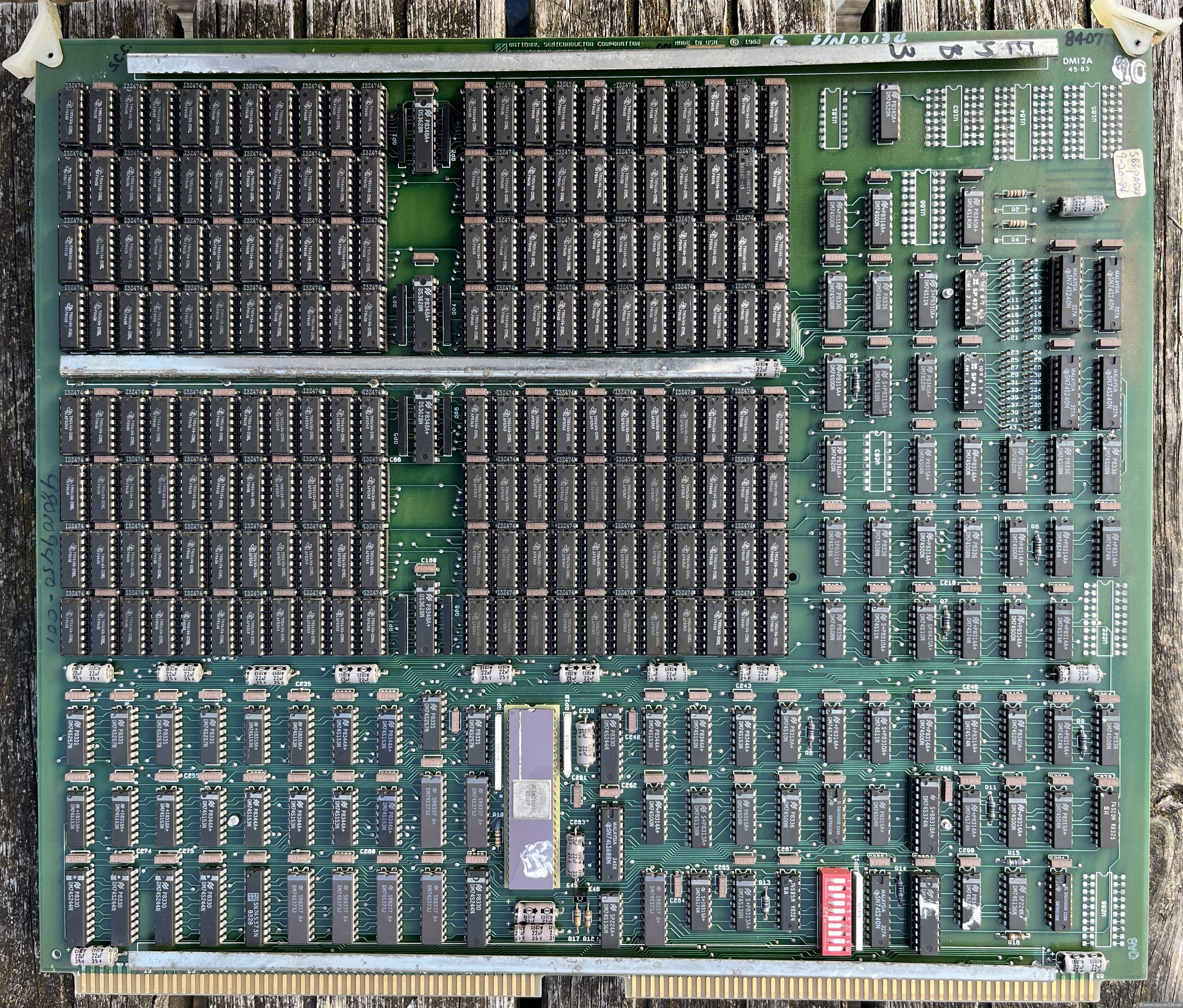
"SECDED" means "Single-Error-Correction-Double-Error-Detection". This technique improves the reliabillity of a system a lot. But it requires more memory and logic chips and is therefore only found in more expensive machines. The 16-bit databus of SYS-16 requires 6 additional bits - an increase of 37% more memory chips for a total of 176 DRAMs on the board. The DRAMs are 64-kbit chips.
The AM2960 EDC in a 48-pin package is the central logic chip. It is described as a "16-Bit Cascadable Error Detection and Correction" device built in bipolar technology.
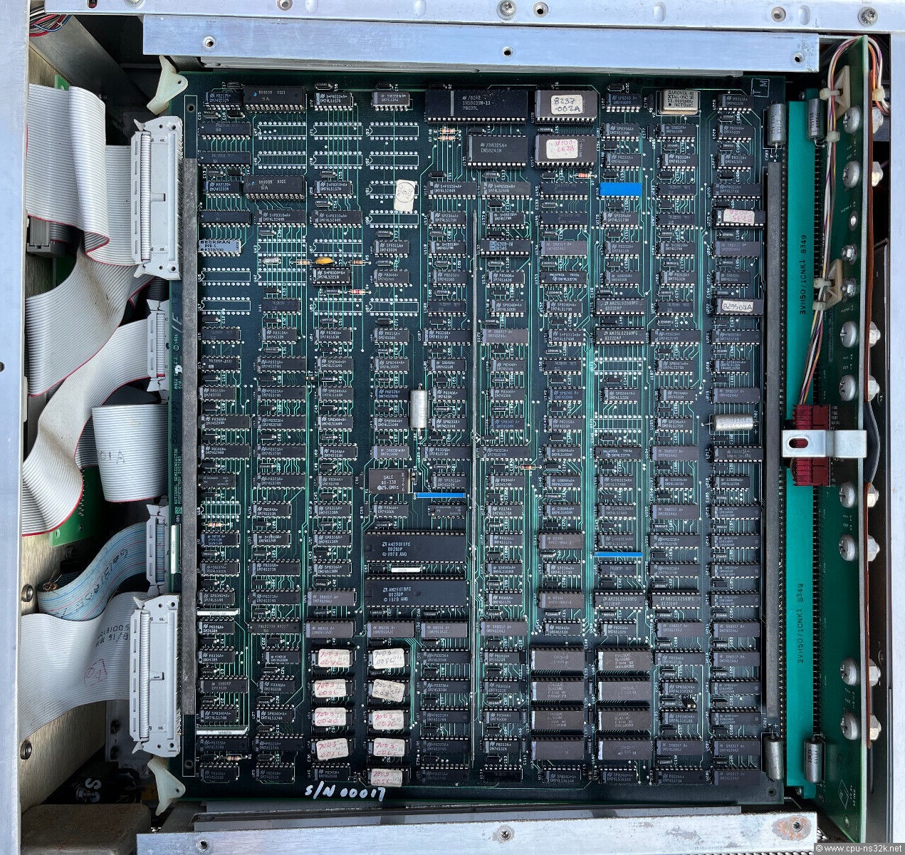
Fig. 38. The disk and tape controller is placed in the first (or last) socket on the backplane.
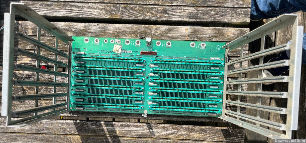
Fig. 39. This photo shows the carrier box for the six boards made of two holders and the backplane.
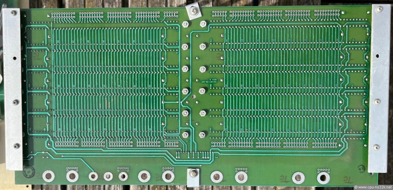
Fig. 40. This is the backside of the backplane.
Thanks to Ian for the great photos.
This chapter was last modified on 5 November 2025. Next chapter: Opus