TSMC 16nm FinFET
TSMC is since many years the leading manufacturer of logic ICs in the world. Only a limited number of companies have the money to compete in the technological race with TSMC. The chip designs of companies like Apple, Nvidia and many others are build by TSMC.
In 2024 I saw the opportunity to synthesize parts of my M32632 in a modern technology. The person I asked was working on an ASIC to be build in the 16nm FinFET process of TSMC. FinFET is state of the art in 2025 with the gate of the transistor covering three sides of the channel. For the synthesis process only some inputs are needed:
- the library of cells, i.e. NAND, NOR, ... in different drive strenghts,
- the clock speed of the design,
- the fill factor of the area, which is the relation between the cell area and the total area
- and the high level description of the design.
The fill factor also allows the delay estimation for the wiring which can be a substantial part of the cycle time. To keep things simple I choose for a first test the opcode decoder of the M32632. It contains also the control state machine. The functionality is pure logic. The fill factor was set to 50%. The design has only one clock which was set to 1.25 GHz = 800 ps cycle time. The result was:
- clock speed target achieved,
- area is 4432 µm².
Wow! The area is only a square with a 67 µm edge. If you have a monitor with 380 dpi resolution, one pixel has the same size.
After this very positive result I wanted more. I choose the double-precision floating-point datapath. This block uses some hard macros of the FPGA to realize a 53 bit by 53 bit multiplier. In the verilog description this is only one line of code. The result was:
- clock speed target not achieved, but well above 1 GHz,
- area is 11181 µm².
For me it is a surprise that the big multiplier works at 1 GHz. Figure 1 shows the chain of gates which are necessary to create a certain result bit: the chain is amazing short. There must be some clever design tricks used to short the path through 52 additions to just 24 gates...
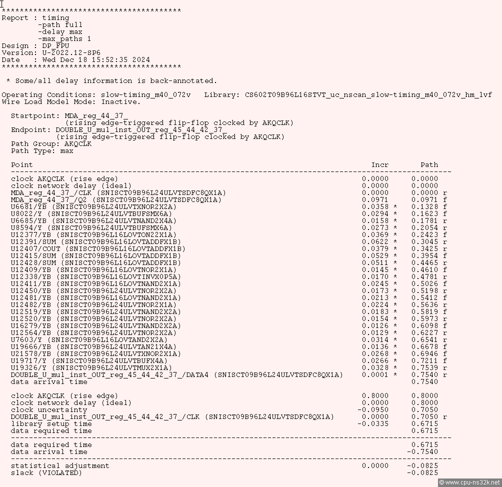
Fig. 1. The listing shows one of the paths which violates the target cycle time. Times are give in nanoseconds.
The numbers in the listing are very impressive. For example the gate U16279 (which seems to be a simple NAND gate with two inputs) has a delay of only 12.6 ps. This is for a 16nm technology. Today the semiconductor industry is delivering chips build in 4nm and even less.
The next step was planned to include a register file. But the time line of the project of the colleague stopped this idea. At the end I'm pretty sure that the area for the complete M32632 would be well below 1 mm².
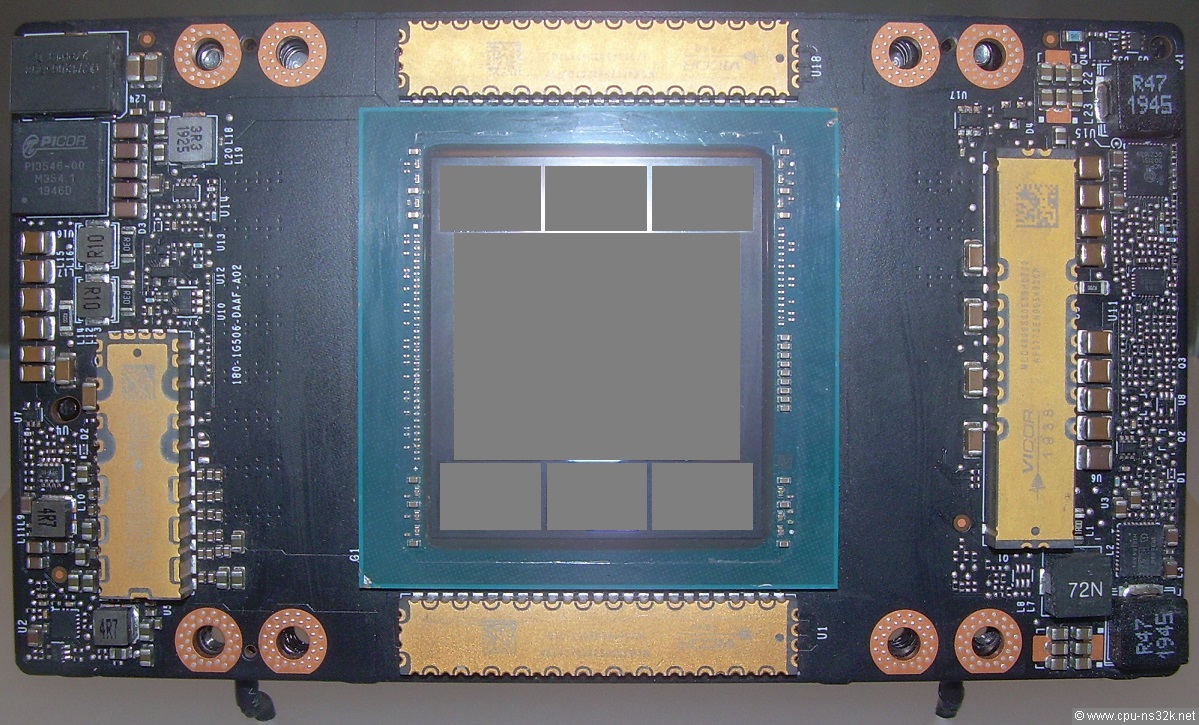
Fig. 2. The big chip in the center of the image is the A100 AI accelarator of Nvidia. The photo was taken at the Deutsche Museum in Munich.
The A100 is a chip with a die size of 826 mm². It is build in 7nm technology and contains 54.2 billion transistors. Such a monster chip could easily contain thousands of M32632, each running at 1 GHz.
From time to time it is necessary to sit back and see what has been achieved in the semiconductor industry since the days of the NS32016...
Next chapter: FLOPUTER