Support Chips
| Device | Date | First Document |
|---|---|---|
| NS16201 | March 1982 | Preliminary Datasheet |
| NS16202 | October 1982 | Preliminary Datasheet |
| NS32203 | February 1986 | Advanced Information |
NS16201/NS32201/NS32C201 TCU
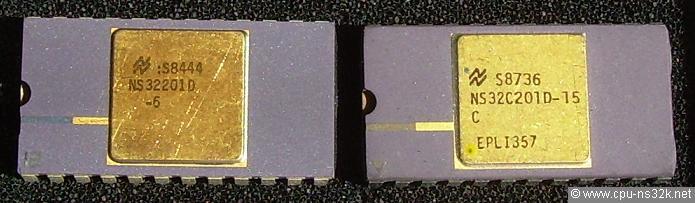
Fig. 1. The NS32201 TCU specified for 6 MHz (left) and the CMOS version NS32C201 for 15 MHz (right) operation.
The NS16201 was the timing control unit (TCU) of the Series 32000 family. The family was later renamed and the TCU became the NS32201. The main task for the TCU was the generation of a full swing two phase non-overlapping clock. For a 10 MHz system clock the TCU uses an oscillator with a 20 MHz crystal. The two phases were needed by the first and second generation CPUs und MMUs. Astonishing both FPUs used only a simple clock signal. This may be one of many reasons for the success of the NS32081 FPU as a floating point peripheral for everybody. The simple clock signal served as the clock source for a computer system.
In addition the TCU served as a wait state generator for the CPU. Wait states are needed if main memory or peripherals are not fast enough to communicate at full speed with the CPU. The first TCU was fabricated on a Schottky bipolar process. This resulted in a high current consumption of 180 mA typical. Later a CMOS version was offered which needed 100 mA typical. All versions used a 24-pin DIL ceramic package.
The third generation CPU, the NS32532, integrated the functionality of the TCU. Driving two high qualitiy clock signals with ever increasing frequencies over pcb traces was no longer feasible.
NS16202/NS32202 ICU
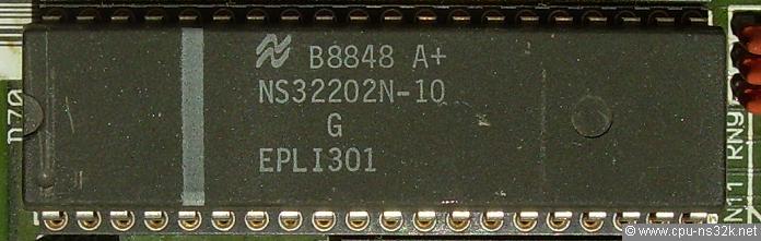
Fig. 2. The NS32202 ICU specified for 10 MHz operation in a plastic package.
The NS16202 ICU was the interrupt control unit of the Series 32000 family. Like the other members of the family it was later renamed NS32202. The most impressive feature was its high price. The chip costs around the same as the NS32016 CPU. But conceptually the ICU was a simple device. It controled up to 16 interrupt sources and contained two 16 bit counters. The CPU itself has only one INT input. In case of an interrupt a special access cycle was performed. The address was 0xFFFE00 (NS32016, 0xFFFFFE00 in NS32332 and beyond) and it was mandatory that at this address an interrupt controller like the NS32202 ICU should be placed. The ICU delivered an interrupt vector to the CPU. In case of an interrupt return a special access cycle informed the ICU that the current interrupt has been serviced.
More than 16 interrupts were possible by cascading multiple ICUs. The maximum number of interrupts was then 128. The ICU was always build in NMOS technology. Due to its low power consumption it was possible to use a plastic 40-pin DIL package.
NS32203 DMAC
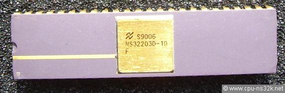
Fig. 3. The NS32203 DMAC specified for 10 MHz operation in a ceramic package.
The NS32203 was a direct memory access controller (DMAC). It was used for transfering data between a peripheral device (for example a printer or a SCSI interface) and main memory without CPU interaction. It was a highly sophisticated device according to the data sheet and could transfer data at a rate of 5 Mbytes per second (10 MHz clock frequency). Four independant channels were available. Each channel could access 16 Mbytes. The chip was build in NMOS technology and used a 48-pin DIL package. I have not seen a system using the device. But this may change in the future :-)
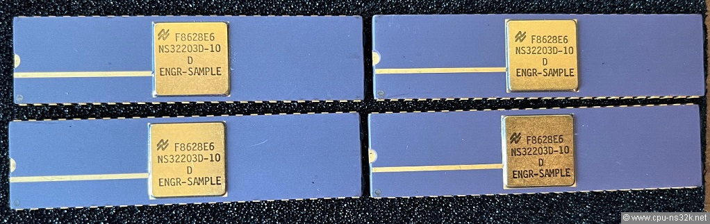
Fig. 3. Another four DMACs which never went into use. Please note the unusual "Engineering-Sample" mark.
This chapter was last modified on 2 September 2023. Next chapter: Second Source