John
John has built an NS32016 system for the S-100 bus. He owns also an Opus board based on the NS32532, see Systems/Opus. He wrote about his projects related to Series 32000:
"Back around 1983-84 I worked for a start-up company in San Diego (Syte Information Technology) who were planning on building a Unix workstation product using the NS32000 chipset. My s/w task was the Fortran compiler for the NS32000, which took about a year to complete. With management issues, and running out of money, the company ceased operation about a year and a half after starting. I am sure you have never heard of them.*)
Knowing nothing about the S-100 bus, but working from the IEEE/ANSI standard and being very impressed with the NS32000 architecture, I got some Vector prototype wire-wrap boards and got to work. ROM was unheard of in those days, so the system had to be bootstrapped from an Apple II. My boot ROM was a battery backed 8K SRAM chip, loaded from the Apple II. My NS32000 assembler and linker were written in UCSD Pascal and ran on the Apple also. The memory board originally had 8K SRAM chips, but knowing the 32K SRAM was just around the corner, you will note the plug on the board which crosses address lines appropriately. With 32K chips the memory became 512K. Serial I/O was using 4 8250 UARTs, two of which have been cannibalized in the attached photo for more recent projects. The NS32016 runs perfectly well; I have played with floating point; but have never turned on the MMU.
I don't know how I found the NS32532 board, but in the late 80s I was aware that the 32000 had gone through 2 major CPU revisions: 32016/32032 originally; 32332; and then the 32532, which finally integrated a decent MMU on the CPU chip. I bought the Opus board from an on-line seller, who provided all the MSDOS utilities to bootstrap it, and all of the System V disks which ran on the board. I note that the 32381 FPU adds a couple of nice polynomial instructions, and extends the chip to 8 x 64-bit floating point registers."
*) Correct.
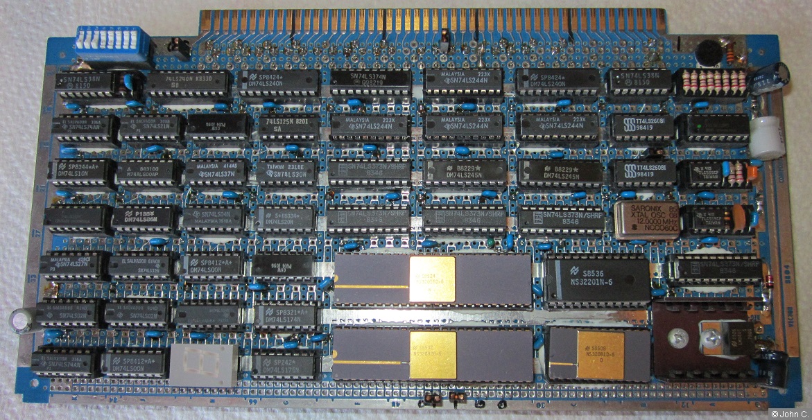
Fig. 1. The CPU board for the S-100 based system. The 5V supply voltage is always generated locally. The regulator with the heatsink is located in the lower right corner.
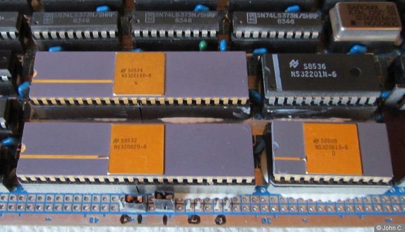
Fig. 2. The Series 32000 CPU cluster running at 6 MHz. The NS32201 TCU uses a plastic package.
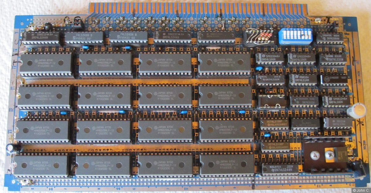
Fig. 3. The memory board for the S-100 based system. The 120 ns SRAM devices from Hitachi are very fast for a 6 MHz system.
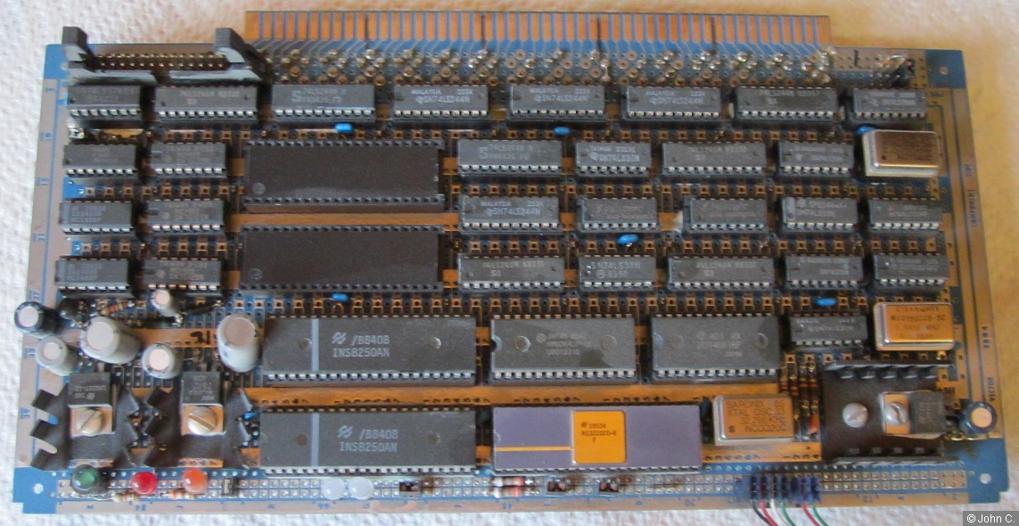
Fig. 4. The serial I/O board for the S-100 based system. A lot of dust can be seen on some of the devices...
Three quartz oscillators are used on the serial I/O board. The 32.768 kHz is used for the real-time-clock HD146818, the 1.8432 MHz is used for the baud rate of the serial ports and the 2.0 MHz clock is used for the S-100 bus.
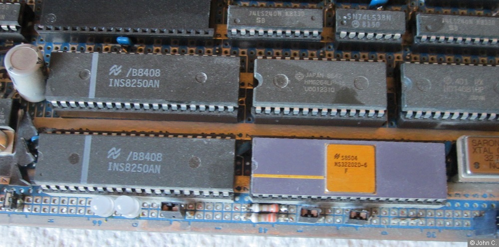
Fig. 5. A detailed view of the serial I/O board. The SRAM HM6264 is the mentioned "ROM" for the system.
The S-100 bus is able to transfer data 16 bits wide. This mode is used for the memory board. The serial I/O board has only an 8 bits wide data port. To fetch data from the "ROM" the CPU is halted until two bytes are loaded. The required functionality for this purpose is the reason for the many TTL chips found on the CPU board.
This chapter was last modified on 16 June 2017. Next chapter: Jon