Udo : TITAN1
I build my first NS32000 CPU board in 1985. All my systems were called TITAN with a number behind to name the generation. The first generation used a 6 MHz set of devices. In figure 1 the board is shown. From left to right the NS32081 FPU, the NS32082 MMU, the NS32016 CPU and the NS32201 TCU can be seen. The NS32202 ICU is placed on an I/O board. Later I upgraded the system to 10 MHz clock frequency. The board contains in addition to the CPU cluster one 16L8 PAL chip for address decoding, some control logic and buffers for the system bus.
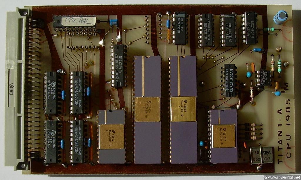
Fig. 1. Top view of TITAN1 CPU board.
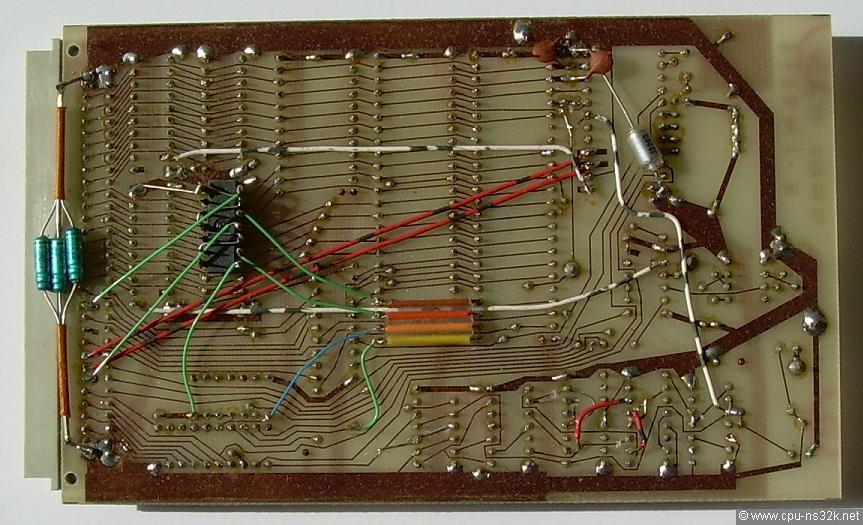
Fig. 2. Bottom view of TITAN1 CPU board.
Another important part of the system is the main memory. My design has 512 kbytes DRAM build with 256-kbit chips. In 1986 this was a lot of memory. The databus was wire-wrapped because I found no way through for it with only two layers of routing.
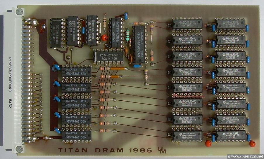
Fig. 3. Top view of TITAN1 memory board.
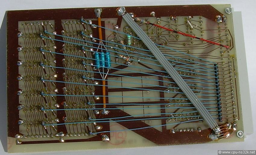
Fig. 4. Bottom view of TITAN1 memory board.
In the 1980's I used foils to create the masks for the photo resist coated PCB. Figure 5 shows together the foils for the top and bottom side of the TITAN1 memory board.
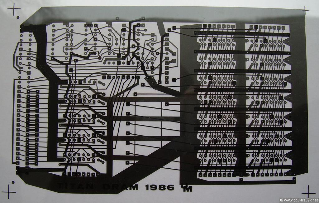
Fig. 5. The foils used for the TITAN1 memory board.
The system is no longer functional. The CPU board now hangs on the wall as an eye-catcher.
TITAN2
The second generation of my CPU boards was developed in 1999. I used the NS32532 CPU and the NS32381 FPU for it. Due to the wire-wrap technology the board runs only at 10 MHz. But I have to say that I never tried a higher speed. Look at the bottom side and you know why. The board is equipped with 16 Mbytes of EDO DRAM. Two ispLSI1016 CPLDs from Lattice are used for the control logic. The interrupt control unit NS32202 of the Series 32000 family is no longer used. Their 40 pin DIL package was too big for the new design. For the CPU and FPU I use ZIF (Zero-Insertion-Force) sockets for easy replacements.
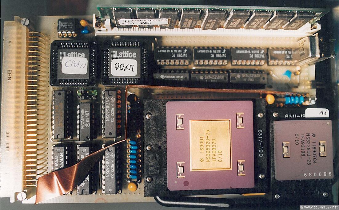
Fig. 6. Top view of TITAN2 CPU board.
The bottom view of the board shows the confusing wires. Keep in mind that the NS32532 has separate 32 bits wide data and address busses. I will never do again such a work!
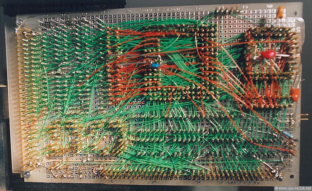
Fig. 7. Bottom view of TITAN2 CPU board.
The system is still functional but not in use any more.
TITAN3
The third generation of my CPU boards was developed in 2005. Again it is based on the NS32532/NS32381 duo. Finally I used modern PCB technology. I created the board with the EAGLE layout software. The board uses 4 layers. The two outer layers are used for signals and figure 7 shows a screen shot of them. Red is the top layer and blue is the bottom layer. The inner two layers distribute all the power and ground. This board is able to run the CPU and FPU at 25 MHz. An ACEX EP1K100 FPGA from Altera having around 5000 logic elements houses all the glue logic of the system. But the main advantage of this FPGA is its 5V tolerant I/O. Therefore the design needs no buffers. All the following generations of FPGAs can only be used in 3.3V systems. DRAM is 16 Mbytes again. For such a system this amount of memory seems to be absolutly sufficient. Only for the CPU I still use a ZIF socket. The smaller FPU uses a standard socket.
I had not expected to use the ZIF socket very often. But the first two CPUs I wanted to use were failing. One had a defect in the TLB of the MMU function. The other one always sets the F-flag during a CHECKB opcode. Finally the third CPU was fully functional. I still have some more CPUs. But one day the party will be over ...
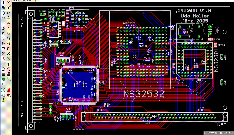
Fig. 8. EAGLE layout view of TITAN3 CPU board.
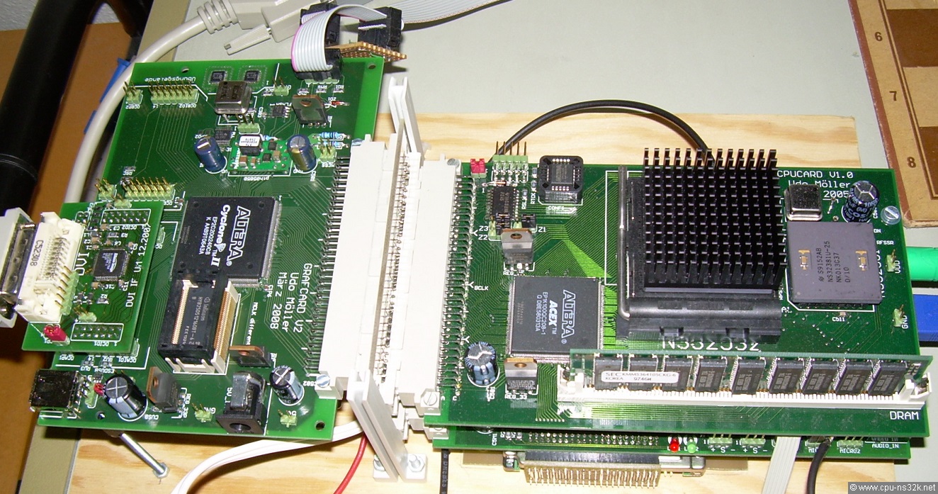
Fig. 9. The complete TITAN3 system: the IO board is placed below the CPU board.
The photo in Figure 9 shows on the left the graphic board. A Cyclone II FPGA from Altera holds the logic. The graphic memory is made of a 64 Mbytes DDR-DRAM. The DRAM has a 16-bit wide data bus and is running at 100 MHz. The bandwidth of 400 MB/s is enough for a 24-bit color mode at a resolution of 1024 by 768 pixels. The interface to the monitor is using a DVI chip from Silicon Magic.
Another photo of the CPU board is shown in the chapter PC532E which reuses the TITAN3 CPU board.
TITAN5
The fifth generation of TITAN is based on a Cyclone V GX FPGA. This FPGA comes in a development kit from Terasic (for more details see the chapter M32632/TRIPUTER). Since TITAN2 the operating system of my computer uses a CAM device. CAM means "Content-Addressable Memory". This is a memory device which puts data in and delivers the address where the data is stored. Data width is 64 bits and the depth of the MUC9C2480A from MUSIC is 2048 words. One can use the address as an index in another table. My software use this mechanism for the assembler, the operating system and the disk cache.
The astonishing fact about CAM is that in 2022 one can not buy such a device. There is no manufacturer any more. In 1997 MUSIC was the first company to offer such a memory. Their main use was in address translation for Ethernet. I believe that the functionality is today integrated in the big ASICs for switches and routers.
To enable TITAN5 on TRIPUTER I had to connect the CAM to the Starter Kit. I designed a small pcb for the expansion connector, see the Figure below. In addition the board contains a small CPLD which does some pin multiplexing and translates 3.3V (TRIPUTER) to 5V (CAM).
I have four CAM chips. All are doing well. But if the last one gets broken, I have to rewrite my OS ...
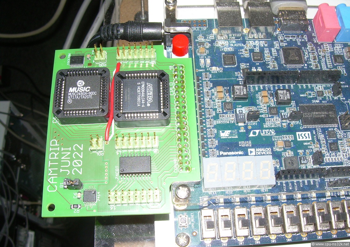
Fig. 10. The CAMTRIP board is connected to the Cyclone V GX Starter Kit through a 40 pin expansion connector.
This chapter was last modified on 22 October 2022. Next chapter: Unknown System