Introduction
The story of Series 32000 began in the late 70's of the last century. It went on full steam throughout the 80's. And it ended sometime in the beginning of the 90's. Today nothing remembers to the Series 32000. It's now more of an archaeological task to find facts and remaining items. Even the company National Semiconductor has disappeared. It was bought in 2011 by Texas Instruments.
In the beginning the name of the product family was NS16000™. Due to difficulties in naming different CPU versions the name was changed in May 1984 to Series 32000™. Both names were trademarks of National Semiconductor.
The first members of the NS16000 family were designed in Herzlia, Israel. Later some CMOS parts of Series 32000 were designed at the headquarter of National Semiconductor in Santa Clara, California/USA.
In 2008 some managers of the Series 32000 came together and talked about what was going on at National Semiconductor in the mentioned period of time. The very interesting discussion took place at the Computer History Museum in Mountain View, California/USA. The record of it can be found here:
Series 32000 History (© Computer History Museum)
It is interesting to read what was a hot topic in the newsgroups in 1986. Google saved a lot of the old ones and made them available through the web. The newsgroup net.micro.ns32k can be found here: https://groups.google.com/forum/#!topic/net.micro.ns32k .
In August 2017 Michael sent me electronic copies of some very old documents from National Semiconductor about NS16000. Among them is "THE NS16000 MICROPROCESSOR FAMILY SYSTEM OVERVIEW REVISION A" from NOVEMBER 15th, 1979. Wow - I have never seen an earlier document than this!
To get an impression about what was planned and later implemented please have a look at THE NS16000 MICROPROCESSOR FAMILY.
The 8080 Emulation Feature
This planned feature was really strange. There was always a rumour about an 8080 emulation mode. Now I see this feature in the document from 15 November 1979:
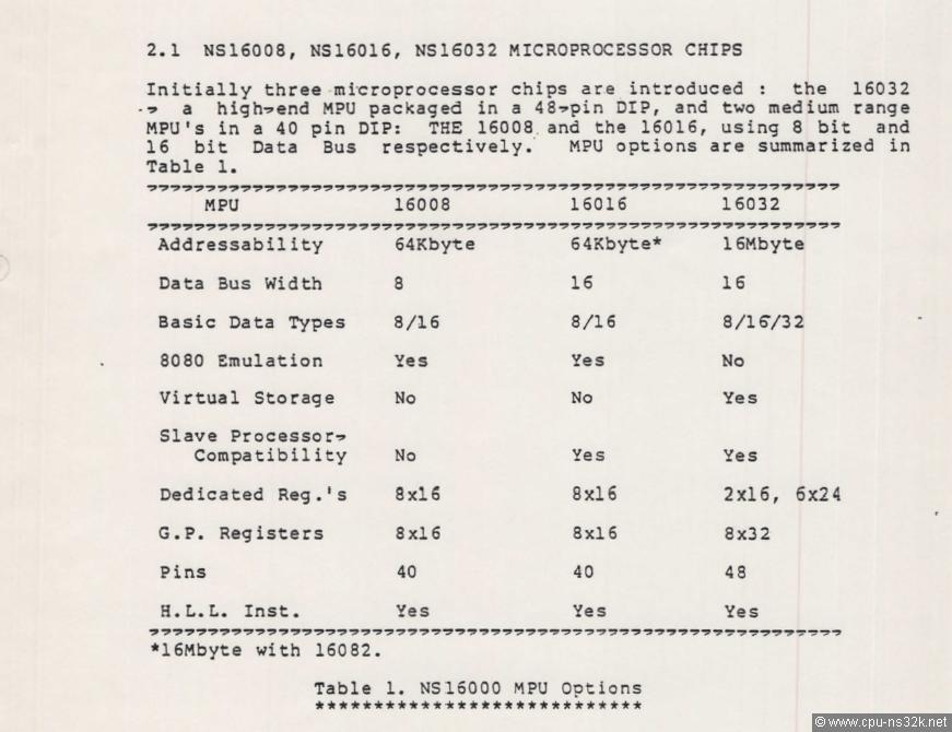
Fig. 1. The first three planned microprocessors: only the NS16032 was built.
The two smaller versions NS16008 and NS16016 should have the 8080 emulation feature. But these processors were not realized. I assume that there was simply no market for them... or no development ressources were available.
But this stop didn't eliminate the 8080 emulation feature from someone's wish list. A document from 15 September 1980 named "NS168032 MICROPROCESSOR TARGET - SPECIFICATTIONS REVISIONS A0" showed the second approach:
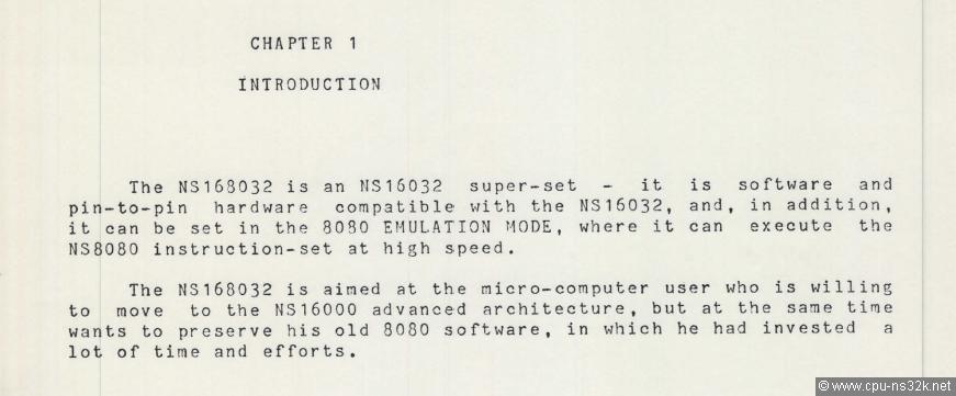
Fig. 2. A new version of NS16032: the NS168032 including the 8080 emulation feature.
The complete document is available here: NS168032 TARGET SPECIFICATIONS. For me it is not clear why this feature should be implemented in hardware. The instructions of NS16032 are so powerful that a software simulator for such a simple processor like the 8080 is easy to implement. On the other side any additional hardware on the chip will be a challenge for the design team. I believe that at the end everybody agreed that this feature is useless.
It is interesting to see the defined instruction set as of 18 August 1980: INSTRUCTION SET. Some instructions have not their final names.
One remark about the microprocessor table in Figure 1: I don't believe that National Semiconductor had an NS32032 in mind at that time. For me it looks as if they were surprised by market developments (MC68020) and then decided quickly to build an NS16032 with a 32-bit data bus - obviously the most simple solution. But not the best solution for their customers...
Before I move on to the technical heart of Series 32000 let's have a look at the following photo. It shows the first devices of Series 32000. They can be easily recognized in their ceramic packages with the golden cap.
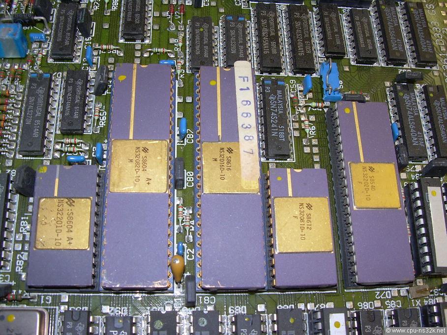
Fig. 3. The complete chip-set of the first generation of Series 32000 devices.
Figure 3 shows from the left to the right all the required chips in ceramic packages to implement the Series 32000 architecture : Timing Control Unit NS32201 (TCU, 24 pins), Memory Management Unit NS32082 (MMU, 48 pins), Central Processing Unit NS32016 (CPU, 48 pins), Floating Point Unit NS32081 (FPU, 24 pins) and Interrupt Control Unit NS32202 (ICU, 40 pins). This was the great advantage of National Semiconductors entry in the high performance microprocessor market : a complete chip set based on an advanced architecture covering every aspect of a modern computer system.
Architecture
This chapter describes the basic architecture of the Series 32000 family. More details can be found in the datasheets of the NS32532 CPU and NS32381 FPU. They can be downloaded in the chapter Chips/Documents.
The architecture of the Series 32000 is based on CISC principles (for more details see the chapter M32632/Performance). Beginning of the 1980's the most popular minicomputer using CISC was the VAX family from Digital Equipment. Undoubtly their success had a great influence on the microprocessor designers of that age.
The Series 32000 architecture is a 32-bit architecture. Registers inside the different CPUs used for integer operands and address pointers were all 32 bits wide. Due to limitations in technology the first CPU generation used only the lower 24 bits for external addresses (16 Mbytes address space).
The difference between the many architectures invented during this time was the amount of exceptions to the basic rules. For example the MC68000 from Motorola is able to add any two operands with every addressing mode by the opcode ADD . The same is not true for add with carry. The opcode ADDX can use only registers or external memory with predecrement address pointers. National makes no exceptions for this two opcodes ADD and ADDC : every addressing mode is allowed in any combination. The advantage is that compilers can be made less complex with less exceptions. I think that the chip design can be made simpler too.
Figure 4 shows the registers of the different functions of the Series 32000 architecture. The register set shown is based on the NS32532 CPU and NS32381 FPU.
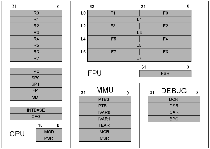
Fig. 4. The registers of the Series 32000 architecture.
Basic Register Set
Every CPU of the Series 32000 family implements the basic register set. This set is used for integer variables, address pointers and control bits.
| Name | Width | Description |
|---|---|---|
| R0 .. R7 | 32 | 8 working registers for integer operations |
| PC | 32 | Program Counter |
| SP0 , SP1 | 32 | Two stack pointers |
| FP | 32 | Frame Pointer, used as address pointer |
| SB | 32 | Static Base, used as address pointer |
| INTBASE | 32 | Interrupt vector table base pointer |
| MOD | 16 | Module register, base address of current software module |
| PSR | 16 | Processor Status Register |
| CFG | 32 | Configuration register |
Debug Register Set
The following register table is based on the debug features of the NS32532 CPU. Earlier CPUs of the family had no debug features. The debug capabillities were integrated in the external MMUs.
| Name | Width | Description |
|---|---|---|
| DCR | 32 | Debug Condition Register |
| DSR | 32 | Debug Status Register |
| CAR | 32 | Compare Address Register |
| BPC | 32 | Breakpoint Program Counter |
MMU Register Set
The following register table is based on the MMU inside the NS32532 CPU.
| Name | Width | Description |
|---|---|---|
| PTB0 , PTB1 | 32 | Two Page Table Base Pointers |
| IVAR0 , IVAR1 | 32 | Two Invalidate virtual address registers |
| TEAR | 32 | Translation Exception Address Register |
| MCR | 32 | Memory Management Control register |
| MSR | 32 | Memory Management Status register |
FPU Register Set
The following register table is based on the NS32381 FPU. National Semiconductor made a big change when they increased the number of 64-bit floating point registers from 4 in the NS32081 to 8 in the NS32381. SP means "Single Precision" and DP means "Double Precision".
| Name | Width | Description |
|---|---|---|
| F0, L0 | 32 | SP Register 0, Lower Double Word of DP Register 0 |
| F1, L0 | 32 | SP Register 1, Higher Double Word of DP Register 0 |
| L1 | 64 | DP Register 1 |
| F2, L2 | 32 | SP Register 2, Lower Double Word of DP Register 2 |
| F3, L2 | 32 | SP Register 3, Higher Double Word of DP Register 2 |
| L3 | 64 | DP Register 3 |
| F4, L4 | 32 | SP Register 4, Lower Double Word of DP Register 4 |
| F5, L4 | 32 | SP Register 5, Higher Double Word of DP Register 4 |
| L5 | 64 | DP Register 5 |
| F6, L6 | 32 | SP Register 6, Lower Double Word of DP Register 6 |
| F7, L6 | 32 | SP Register 7, Higher Double Word of DP Register 6 |
| L7 | 64 | DP Register 7 |
| FSR | 32 | Floating Point Status register |
Addressing Modes
The "Top of Stack" (TOS) addressing mode is the only one which includes auto-increment and auto-decrement capabillity. For data movements from one location to another a powerful set of string instructions is available. The index modes can be used only once in a memory access.
| Mode | Assembler Syntax | Effective Address (EA) |
|---|---|---|
| Register 0 .. 7 | R0,F0,L0 .. R7,F7,L7 | None: Operand is in the specified register |
| Register 0 .. 7 relative | disp(R0 .. R7) | Disp + Register |
| Frame/Stack/Static memory relative | disp2(disp1(FP/SP/SB)) | Disp2 + Pointer, Pointer = Disp1 + Register |
| Immediate | value | None: Operand is input from the instruction queue |
| Absolute | @disp | Disp |
| External | EXT(disp1) + disp2 | Disp2 + Pointer, Pointer is found at Link Table Entry number Disp1 |
| Top of stack | TOS | Top of current stack, either SP0 or SP1 |
| Frame/Stack/Static memory | disp(FP/SP/SB) | Disp + Register |
| Program memory | * + disp | Disp + PC |
| Index, bytes | mode[Rn:B] | EA(Mode) + Rn |
| Index, word | mode[Rn:W] | EA(Mode) + 2 * Rn |
| Index, double words | mode[Rn:D] | EA(Mode) + 4 * Rn |
| Index, quad words | mode[Rn:Q] | EA(Mode) + 8 * Rn |
NS32532 Comparison to other CPUs
The table compares popular 32 bit CISC microprocessors at the end of the 1980's with their key characteristics. It can be seen that the designs were very similar.
| Feature | NS32532 | MC68030, Motorola | i80386, Intel |
|---|---|---|---|
| Data Width | 32 bit | 32 bit | 32 bit |
| Address Space | 4 GByte | 4 GByte | 4 GByte |
| MMU | on chip | on chip | on chip |
| Data Cache | 1024 Byte | 256 Byte | 0 |
| Instruction Cache | 512 Byte | 256 Byte | 0 |
| Maximum Clock | 30 MHz | 50 MHz | 33.3 MHz |
| External FPU | NS32381 | MC68881 | i80387 |
Second Silicon
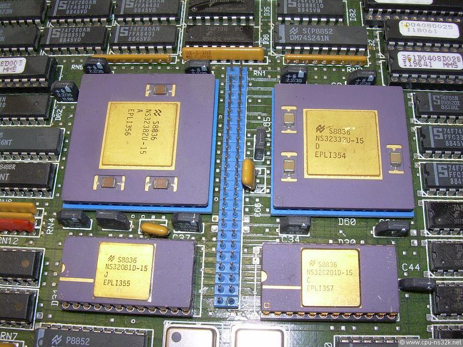
Fig. 5. A chip-set mixing second and first generation Series 32000 devices.
Figure 5 shows a mixed chip-set : the NS32332 CPU and the NS32382 MMU are second generation designs. The NS32081 FPU is from the first generation. The main difference between the second and the first generation was the introduction of a 32 bits wide external address bus. This requires a bigger package for the CPU and the MMU. The traditional DIL (dual in line) packages were replaced by PGA (pin grid array) packages. Another advantage was the use of decoupling capacitors directly soldered on the package for very low inductance. This was the first sign that high speed semiconductor devices need special service for reliable operation. Note the increased clock frequency of 15 MHz compared to 10 MHz of the first generation.
This chapter was last modified on 20 August 2017. Next chapter: CPUs