Memory Management Units (MMUs)
| Device | Date | First Document |
|---|---|---|
| NS16082 | March 1982 | Preliminary Datasheet |
| NS32382-15 | February 1986 | Advanced Information |
NS16082/NS32082
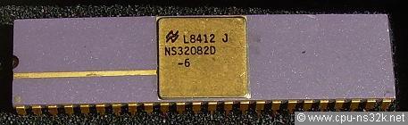
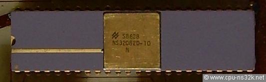
Fig. 1. The NS32081 MMU specified for 6 MHz (left) and 10 MHz (right) operation.
The NS16082 MMU was the first generation memory management unit of the Series 32000 family. It was called NS16082 when it appeared on the market and was later renamed to NS32082. It could be used together with the NS32016 and the 32-bit version NS32032 to create systems with virtual memory support. The main task of a MMU is address translation. A so-called "virtual address" coming from the CPU is translated by the MMU to a "real address" and then used in the system. The address bits 23 downto 9 are being replaced. The bits 8 downto 0 are unchanged. Therefore the "virtual page size" of the NS32082 was 512 bytes. The translation tables are stored in main memory.
But if every access must first access this tables in memory then the system would be slowed down dramatically. The solution is to store the last 32 address translations in a fast buffer inside the MMU. Every virtual address is compared against the 32 addresses stored (fully associative). If a "match" (or "page hit") occurs the stored real address is immeaditly driven on the address bus. If there is no match (a "page fault") the MMU is able to access the translation table in main memory and to update its internal 32 entry buffer.
The CPU is not being informed about the work of the MMU. For the CPU the access simply needs more clock cycles. If there is no valid translation in the table in memory then the MMU is "aborting" the access from the CPU. For the CPU the "abort" trap has a higher priority than any interrupt inclucding the "non maskable interrupt" (NMI). Therefore the CPU is forced to correct the situation. After a successful correction the aborted instruction is executed again.
This translation process can be expanded by useful protection mechanism. For example a page can be marked as read-only. If a program tries to write into this page an abort occurs. Unfortunately by today's perspective National Semiconductor did not see the necessarity of an execute-only page flag. In the beginning of the 1980's the computer world had not yet invented angry programs.
The NS32082 had a 16 bits wide databus and worked as a coprocessor to the CPU. If the CPU executed the opcodes LMR (Load MMU Register) and SMR (Store MMU Register) it accessed registers inside the MMU chip which were used to control the process of address translation. In addition all MMUs provided some debug capabillities. For example an address register is compared to all addresses coming from the CPU. If a match is detected an interrupt occurs (abort is used by the NS32382 MMU). This is helpful for program debugging. The NS32082 was build into a 48-pin DIL ceramic package with a nearly identical pin out like the NS32016 CPU. Therefore both devices could be placed very close to each other on a pcb. It was build in 3.5 µm NMOS technology, required approximately 20,000 transistors on a 6.8 * 6.8 mm² = 47 mm² die and achieved a maximum clock frequency of 10 MHz like the supported CPUs.
NS32382
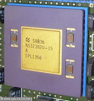
Fig. 2. The NS32382 MMU specified for 15 MHz operation.
The NS32382 MMU was the second generation memory management unit of the Series 32000 family. This chip was also the last separate MMU chip. Advances in semiconductor manufacturing allowed more transistors on one chip and the MMU was the first Series 32000 coprocessor to be integrated on the CPU chip (see NS32532 CPU). Motorola and Intel did the same with their designs.
The NS32382 MMU has been used only with the NS32332 CPU. A great improvement in the Series 32000 architecture was the introduction of a 4 Kbytes page size (address bits 11 downto 0 are ignored in translation). This was recognized as a way to increase performance due to less page table accesses in memory. In addition the amount of memory in computer systems was constantly growing and larger pages allows smaller translation tables in memory. Such a development was not anticipated by the design engineers of the first Series 32000 generation.
The NS32382 MMU featured the same 32 entry fully associative translation look-aside buffer (TLB) like the NS32082. But the register definitions and debug capabillities had changed. Therefore the newer generation was not software compatible to the first generation. The chip was built into a 125-pin PGA package and used NMOS technology. Maximum clock freqency was 15 MHz like the NS32332 CPU.
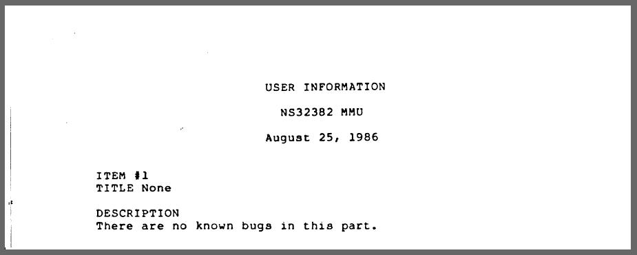
Fig. 3. The User Information of this MMU was very positive for the customer: the NS32382 was the only Series 32000 device which had no bugs in its first silicon!
This chapter was last modified on 2 October 2016. Next chapter: Support Chips