Architecture
The M32632 is not hammered in stone. Every time a new FPGA development board came into use some changes were necessary. For example the Cyclone V GX Starter Kit has a high DRAM bandwidth due to its LPDDR2 device. This required a new DRAM interface. The read data bus is now 128 bits wide which is a full cache line. In addition some bug fixes are inlcuded in each new version.
This chapter gives an overview of the external connections to the M32632 Version 3.0 .
Top Level View
In Figure 1 the symbol of the M32632 CPU can be seen. The symbol is used in Altera's design software when you create a system in which the CPU is a component. The pins on the left side are all input pins and the pins on the right side are all output pins. Normally all of this pins are not directly connected to real I/Os of the FPGA. Inside an FPGA no bidirectional connections exists. Therefore a databus has always two components, one for reading and one for writing.
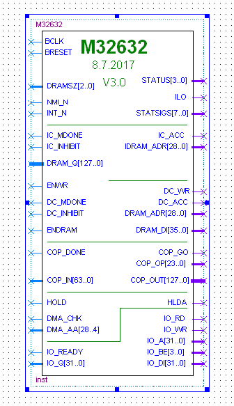
Fig. 1. The symbol of the M32632 CPU.
I/O signals which belong to a certain function are described in the following tables.
Basic Signals
| Signal | Dir | Function |
|---|---|---|
| BCLK | IN | Basic Clock |
| BRESET | IN | Reset synchronized to BCLK |
| DRAMSZ[2..0] | IN | Configuration of DRAM size |
| NMI_N | IN | Non maskable interrupt signal |
| INT_N | IN | Maskable interrupt signal |
| STATUS[3..0] | OUT | Status code for General Purpose Interface |
| ILO | OUT | Interlocked bus cycle |
| STATSIGS[7..0] | OUT | State signals which can be used to monitor CPU activity |
BCLK should be also the system clock.
General Purpose Interface
| Signal | Dir | Function |
|---|---|---|
| IO_RD | OUT | Read access |
| IO_WR | OUT | Write access |
| IO_A[31..0] | OUT | Access address |
| IO_BE[3..0] | OUT | Byte enable signal for write access |
| IO_DI[31..0] | OUT | Data bus used for writing |
| IO_Q[31..0] | IN | Data bus used for reading |
| IO_READY | IN | Acknowledge signal for end of access |
DRAM Interface
| Signal | Dir | Function |
|---|---|---|
| IC_ACC | OUT | Instruction cache read access |
| IDRAM_ADR[28..0] | OUT | Address of instruction cache access |
| IC_MDONE | IN | Acknowledge signal for end of instruction cache access |
| IC_INHIBIT | IN | If active the instruction cache access is not cachable |
| DC_WR | OUT | Write access |
| DC_ACC | OUT | Data cache read access |
| DRAM_ADR[28..0] | OUT | Address of data cache access |
| DC_MDONE | IN | Acknowledge signal for end of data cache access |
| DC_INHIBIT | IN | If active the data cache access is not cachable |
| DRAM_DI[35..0] | OUT | Byte enable signal and data for memory write access |
| DRAM_Q[127..0] | IN | Memory data bus used for writing into the caches |
| ENWR | IN | Enable write signal for the data cache (write buffer empty) |
| ENDRAM | IN | Enable DRAM after system initialization |
The M32632 CPU must be configured to the DRAM size of the system. Currently the CPU can be used with a maximum of 512 MBytes of DRAM memory.
DMA Interface
| Signal | Dir | Function |
|---|---|---|
| HOLD | IN | Hold request signal |
| HLDA | OUT | Hold acknowledge signal |
| DMA_CHK | IN | The address bus DMA_AA is valid |
| DMA_AA[28..4] | IN | DMA address which is currently accessed |
Coprocessor Interface
| Signal | Dir | Function |
|---|---|---|
| COP_GO | OUT | Start coprocessor operation |
| COP_OP[23..0] | OUT | Coprocessor operation code |
| COP_OUT[127..0] | OUT | Data to coprocessor, two 64 bit quad words |
| COP_DONE | IN | Coprocessor has finished operation |
| COP_IN[63..0] | IN | Data from coprocessor, one 64 bit quad word |
System Level View
Today every simple development board for FPGAs has enough DRAM capacity to build a capable computer system. Figure 2 shows a typical system where most of the functions are integrated in the FPGA. The use of a DMA controller is optional.
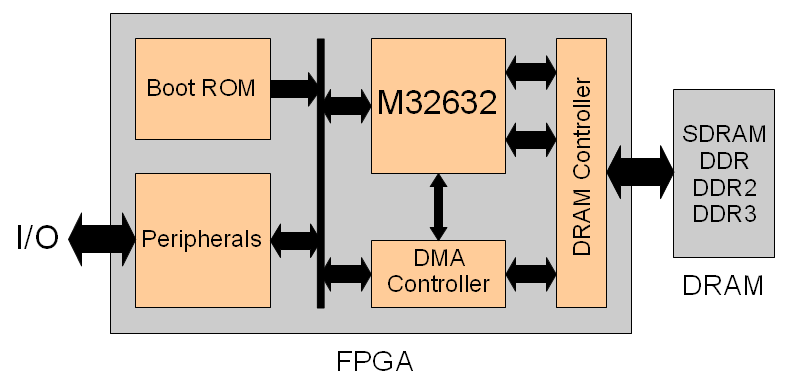
Fig. 2. Computer in an FPGA : the world of today.
Timing Level View
Figure 3 shows the timing of basic I/O cycles. A read access (IO_RD="1") needs two clock cycles if an FPGA memory block is accessed. The reason is that the address is latched inside the memory block and data (IO_Q="00000075") is valid after latching the address. If BCLK is slow the falling edge can be used for latching the address and then the access can be done in one clock cycle. A write access (IO_WR="1") inside the FPGA is done in one clock cycle. The high state ("1") of the signal IO_READY tells the CPU that the access has been finished. External accesses normally require multiple clock cycles.
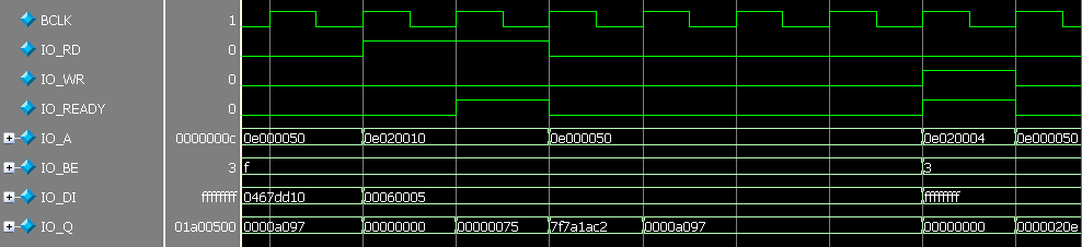
Fig. 3. I/O read and write of the M32632 CPU.
More informations about the M32632 V3.0 and how to build a system with it can be found in the next two documents:
M32632 Version 3.0 Architecture
M32632 Version 3.0 User's Manual
This chapter was last modified on 9 December 2018. Next chapter: Performance