Floating-Point Units (FPUs)
| Device | Date | First Document |
|---|---|---|
| NS16081 | October 1982 | Product Preview |
| NS32310 | 1986 | Only Hints |
| NS32381-20 | October 1987 | Preliminary Datasheet |
| NS32580-30 | April 1988 | Preliminary Datasheet |
| NS32181 | April 1991 | Preliminary Datasheet |
Very early FPU Instruction Sets
In August 2017 I got two very early documents from Michael describing the floating-point instruction set. The first one shows the set as of 30 June 1980 and the second one as of 18 August 1980. Both sets are significant different to the set implemented in the NS16081 FPU.
Remarkable is the abandonment of the instructions SAVEFREG / SVFREG and RESTOREFREG / RSFREG. Doing a save or restore of the complete FP register set with the MOVf instruction is slow because of the slave processor protocol overhead. Maybe the available microcode ROM was to small to implement these instructions.
Some instructions for matrix and polynomial calculations also get lost (DOTx,POLYx). The engineers of National Semiconductor defined a nice variation of them (DOTFL,POLYFL) with two single precision operands as input and a double precision register for the sum. Later the simple forms were included in the NS32381 FPU instruction set.
Two instructions for transforming FP operands were never implemented. INTy / INTf and MOVFRACy / FRACf seemed not to be useful enough for the required transistors.
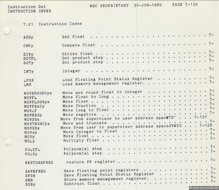
Fig. 1. The FPU instruction set (and the MMU instructions) as of 30 June 1980.
The list in Figure 1 contains some MMU instructions. LMR, SMR, MOVSUx and MOVUSx can only be executed if a system used the NS16082 MMU.
One new instruction appeared in the list of 18 August 1980. The MAGf instruction is very useful and easy to implement. Later it was renamed to ABSf. Obviously the names of some FP instructions changed over time. The list in Figure 2 shows the final names.
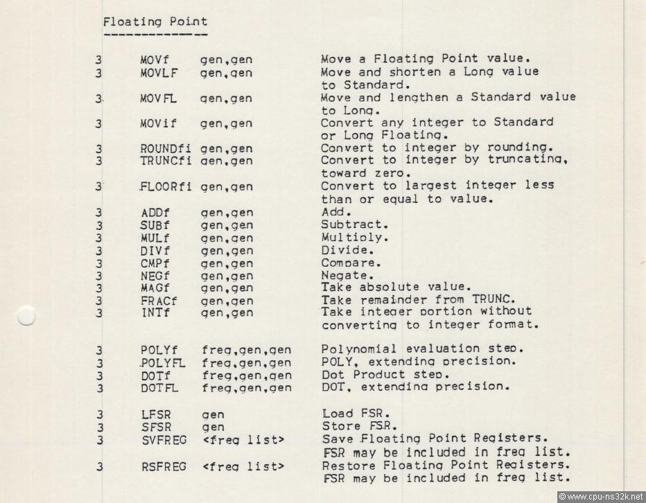
Fig. 2. The FPU instruction set as of 18 August 1980. The names are now final with the exception of MAGf which became ABSf.
NS16081/NS32081
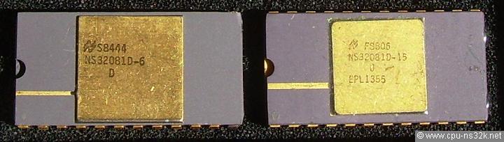
Fig. 3. The NS32081 FPU specified for 6 MHz (left) and 15 MHz (right) operation.
The NS16081 FPU was the first generation floating-point unit of the Series 32000 family. It was called NS16081 when it appeared on the market but was later renamed to NS32081 like the other chips of the family. It offered the four basic arithmetic operations ADD, SUB, MUL and DIV, supports conversions between integer and floating-point operands and had eight 32 bits wide working registers. The basic operations required fom 48 up to 119 clock cycles. Floating-point operand sizes were 32-bit single precision and 64-bit double precision. Rounding modes were compatible to IEEE-754 standard.
The chip was first build into a 24-pin DIL ceramic package. It had a 16-bit databus and used a very simple transfer protocol for opcodes and operands. The transfer rate between CPU and FPU was always 2 clock cycles. A 64 bit double precision operand needed four transfer cycles respectivly 8 clock cycles. The chip was build in NMOS technology and achieved up to 15 MHz clock frequency. Later the chip was offered in a plastic package.
Please note that in Figure 3 the lid size of the 15 MHz version is smaller compared to the older 6 MHz chip. This is an indication for a smaller and therefore faster chip.
20 years later, in 2004, Intel introduced in the Pentium 4E the instruction FISTTP which does the same like the instruction TRUNCfi in the NS32081! It is never to late to learn from the best 😊
Fig. 4. The NS32081 FPU in a plastic package.
The marking of the FPU device in Figure 4 is done with a laser. Please note the unusual date code: week 25 of year 2009! It is not a fake - the chip is functional in an Acorn 32016 Second Processor. Design step information is normally given, but here it is missing.
Because of the simple interface the FPU was not only used with Series 32000 CPUs. AN-383 : Interfacing the NS32081 as a Floating-Point Peripheral describes how to use the FPU with the MC68000 CPU from Motorola. Another reason was that simply no alternative existed. Motorola had no FPU chip for their 16/32-bit processors. The only other FPU of this time the 8087 from Intel could not be used with other CPUs.
Figure 5 shows an example of this usage. The board was made by Hewlett-Packard for its HP 9000 line of computers especially for the ones based on the Motorola MC68010 processor.
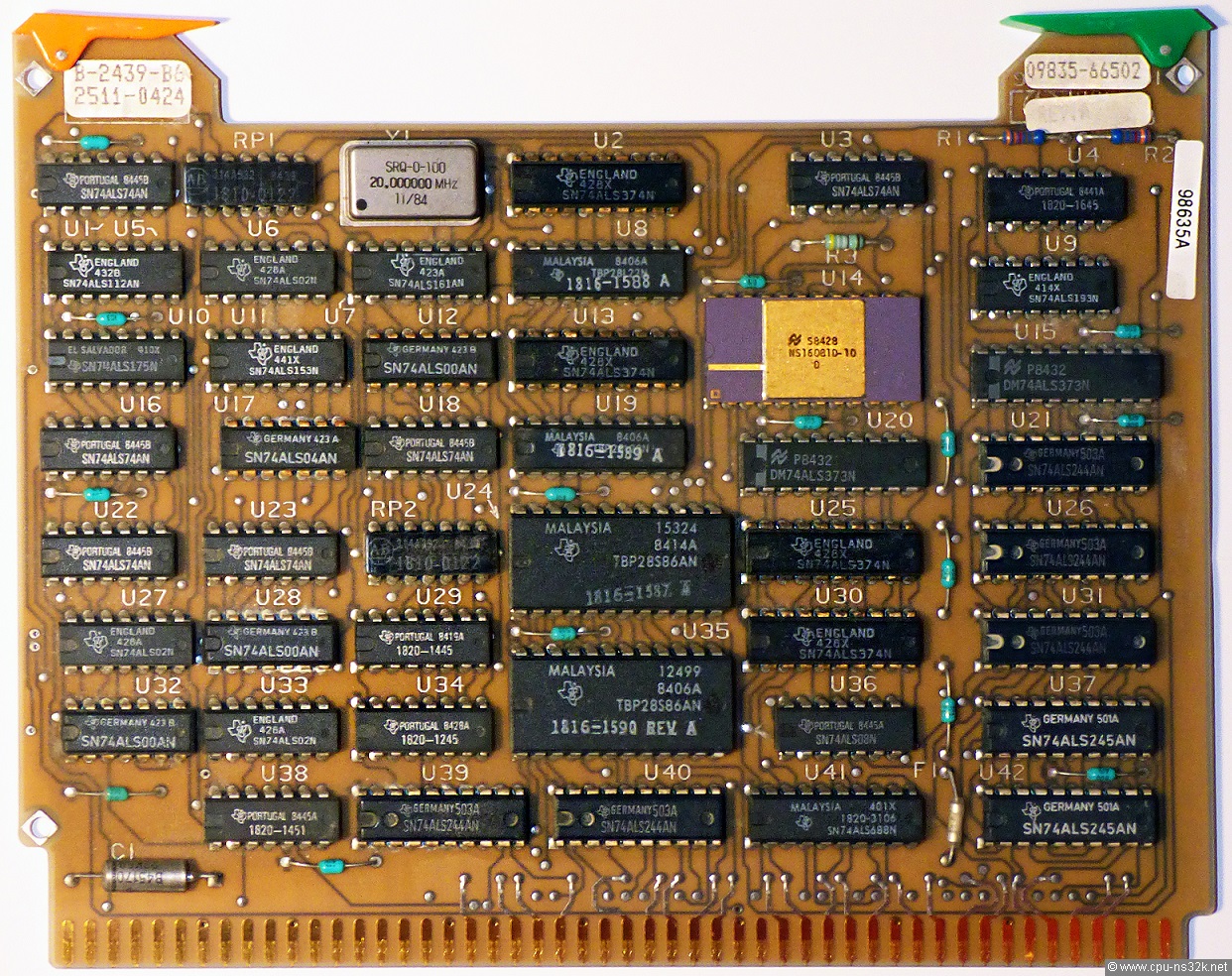
Fig. 5. This accelerator board HP 98635A uses the early NS16081 FPU.
The board in Figure 5 is memory mapped in the address space of the MC68010. The number of chips is much higher compared to the solution in the mentioned application note. Two 1024 x 8bit PROMs TBP28S86AN form a state machine which generates commands for the FPU. HP enhanced their BASIC and Pascal software to make the use of the FPU easy.
Because of the different applications maybe the NS16081/NS32081 was the best-selling device of Series 32000.
NS32081 in a Pin-Grid-Array package
In May 2025 I saw for the first time a photo of the CPU board APC of Encore (see it at Systems/Encore). On the first view I missed the usual FPUs of Series 32000. The second view found something spectacular: an NS32081 in a PGA package! Such a thing was never mentioned in any datasheet or databook.
Fig. 6. The fully unknown device until now: NS32081 in a PGA package.
I asked my contacts at National Semiconductor whether they know something about this version. But all said no. The common opinion is that this version was made because the target device NS32381 for the APC was not yet available. It would very interesting to open one of the two NS32081U to see what is inside...
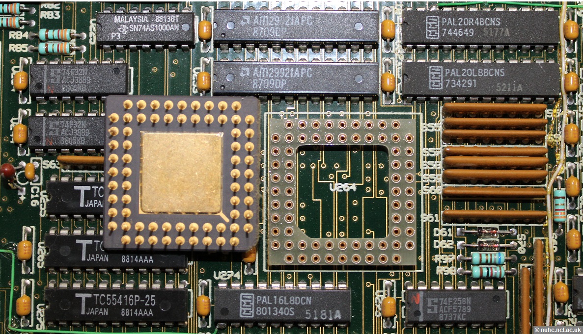
Fig. 7. This beautiful photo shows the backside of the NS32081U FPU together with the socket.
The bottom side of the package of NS32081U is identical to the package of the NS32381 (compare Figures 7 and 8) This supports the mentioned theory that this version was made only for Encore because it was an important customer.
Thanks to John for taking the chip out and for making the great photo.
NS32310
At the end of 1985 National Semiconductor announced a cooperation with Weitek Corp. which was at that time the market leader for high performance floating-point chips. The goal was to develop an interface chip, named NS32310 FPC, to link the Series 32000 family to Weitek's 64-bit floating-point chip set WTL1164/WTL1165. The combination of the three chips would have been more than 10 times faster compared to an NS32081 FPU. The chip was called FPC which means Floating-Point Controller to show that it is not a Floating-Point Unit which includes the data path.
But in the 1986 edition of the Series 32000 databook only in the appendix of the NS32332 CPU a schematic containing the chip set could be found. No advanced datasheet was published although the schematic was detailed. At the end the NS32310 exists only on paper.
NS32381
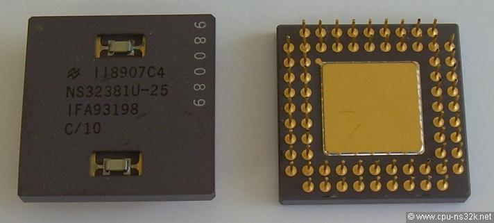
Fig. 8. Frontside and backside of the NS32381 FPU specified for 25 MHz operation.
The NS32381 FPU was the second generation floating-point unit of the Series 32000 family. It could be used with any Series 32000 CPU including the low-end NS32008. The design was making some extensions to the original definition of the Series 32000 architecture. The main change was the increase from four to eight 64 bits wide working registers. The original architecture was stingy with registers due to technology limitations. This chip did the same operations like the NS32081 plus instructions for DOT (A*B + F0) and POLY (A*F0 + B) operations. They perform two floating-point operations (MUL and ADD) in one opcode. Register F0 was fixed for the resulting sum. In addition two new instructions could be used for scaling operands (SCALB and LOGB).
The chip was available in a PGA and a PLCC package each with 68 pins. It was manufactured in CMOS technology. The external data bus width was 32 bits. The internal microarchitecture seems to be similar to the NS32081. More performance comes mostly from the higher clock frequency of up to 30 MHz, not from aggressivly less clock cycles per operation. The chip required for the basic arithmetic operations from 20 up to 59 clock cycles . In addition the 32-bit interface speeded up transfers of opcodes, operands and results between the FPU and the CPU. One transfer took two clock cycles like the NS32081.
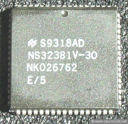
Fig. 9. A 30 MHz NS32381 from 1993 in a PLCC package. I don't know a system using this version of the FPU.
An unknown bug...
In Summer 2026 I was curious about the rumor that the DOTf and POLYf instructions provide greater precision than a combination of MULf and ADDf. This behavior is achived by not rounding the multiplication result which is the first operation in DOTf and POLYf. My FPGA implementation of NS32381 goes the simple way with separate MULf and ADDf operations (sorry for that...) .
POLYf is used very often in the implementation of trigonometric functions. The Savage benchmark is a good test for the precision of these calculations. I run this benchmark and got different results for NS32381 and M32632. To my surprise the result of M32632 showed a little better precision.
Because of this result I wanted to understand how the rounding of DOTf and POLYf was implemented in the NS32381. The datasheet says nothing about this. Even it does not mention a higher precision. But some earlier results pointed in this direction.
The test program used the DOTf instruction and the values 1.0 + 1 LSB and 1.0 - 2 LSBs as the inputs for multiplication. Finally it adds 1.0 . The values were double precision numbers with 64 bits. + 1 LSB and - 2 LSBs modifies 1.0 by the same amount in positive and negative direction.
The result of this calculation shall be something around 2.0 depending on the rounding. But the NS32381 FPU has a very different opinion about the result: 3.0 !
I was shocked. Has this FPU a defect? It would not be the first one. This FPU has a design step of D/10 which is to my knowledge the last revision of NS32381. I tested the calculation on my VME532 system which uses an NS32381 of design step C/10 : the result was the same... (C/10 has a serious bug in the POLYf opcode: if one of the operands is 0.0 the system hangs up! I have verified this 🙁).
Further investigations showed that a wrong result is produced if the operands are 2**n + 2**m LSBs and 2**n - 2*(2**m) LSBs . "n" can be any number, "m" < 26. The wrong result of the multiplication is two times the true result. Obviously a carry bit is wrongly processed.
This bug is not mentioned in the bug sheets I have. There are many possibilities to produce a wrong result. But there are many more correct results. Maybe National Semiconductor did know this bug. But it was not serious enough to produce a new revision of the chip. It is more frustrating that this bug was not already found in the C revision. This shines a bad light on the design verification at National Semiconductor.
NS32580
After the failure of the NS32310 FPC National Semiconductor tried again to develop an interface chip for a Weitek floating-point unit. This time the NS32580 FPC was designed as a coprocessor for the NS32532 CPU. On the other side the FPC was connected to the single chip Weitek WTL3164 Floating-Point Data Path (FPDP) which was doing the real work. The Weitek chip provided the basic arithmetic operations and added the square-root (SQRT) and a multiply-add (MAC) operation as new instructions to the Series 32000 architecture.
This time the cooperation was successful and a detailed preliminary data sheet appeared. The operation of the chip set was specified for up to 30 MHz clock frequency. The data sheet promised up to 15 Mflops peak performance for single and double precision multiplies and additions. The package of the NS32580 was a 172-pin PGA. The technology for this chip was 1 µm CMOS which was more advanced than the technology of the NS32532 CPU.
I looked for a photo of this device for a long time. It was easier to get one for the very rare NS32SF640 CPU. In Summer 2016 I wrote an email to the designer of the chip. He was very kind and said that he must have some devices. In November he wrote that he could not find the chips - not the best message if you are full of hope. But some days later I got a new mail from him - this time containing some photos! What a surprise - he has not given up the search and finally was successful. Shay, thanks a lot for your efforts!
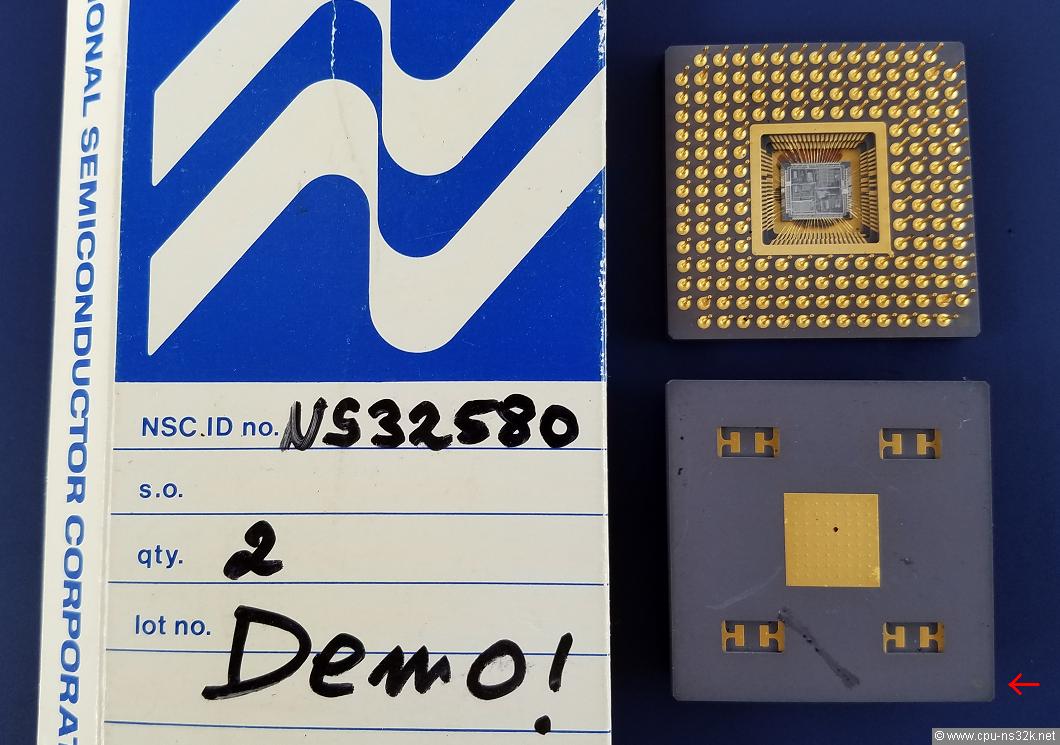
Fig. 10. Top and bottom view of an enginering version of the NS32580. The red arrow is pointing to the very weak pin A1 marking.
NS32181
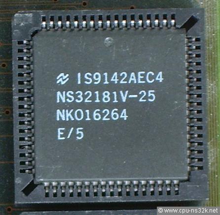
Fig. 11. The NS32181 FPU in a socket of an Indel AG board.
The NS32181 FPU is a 16-bit bus version of the NS32381 FPU. The chip was packaged in a low-cost 68-pin PLCC and the maximum operating frequency was 25 MHz. Both FPUs have the same pinout and the same features. Therefore my assumption is that only one chip was used.
Is it possible that an NS32181 functions as an NS32381? An interesting question. The first condition is that all bond wires exist. Figure 12 shows what is in the plasic package of Figure 11.
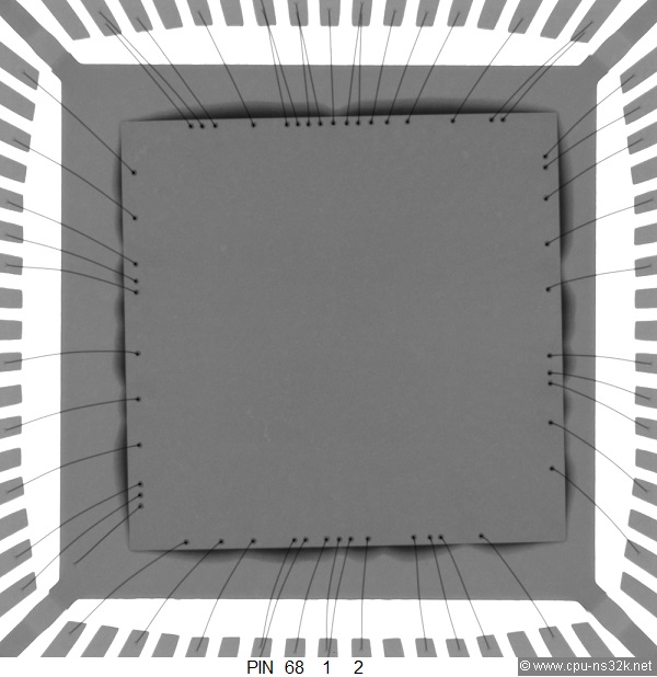
Fig. 12. The X-ray image of the NS32181 FPU shows a lot of missing bond wires.
No chance to replace an NS32381 with an NS32181! National Semiconductor took away the bond wires for the upper 16 bits of the data bus. Nevertheless to see that the same die is used for both chips compare Figure 12 to the die photo of the NS32381 in Chips/Die Photos.
This chapter was last modified on 12 July 2026. Next chapter: MMUs