FPGA
The "Field-Programmable Gate Array" (FPGA) is the holy grail for every digital logic designer. Any digital circuitry can be implemented in such devices. "Field-programmable" describes the most important characteristic of a FPGA : it can be reprogrammed, for example to correct a bug or to implement a new function. For this purpose the FPGA contains from thousands up to millions of flipflop cells which are set to a defined state by a process called configuration. This is normally done after power-up of the system and takes some seconds. But it can also been done at any time, for example during the development process.
FPGAs were invented in 1983 by the company Xilinx. A prominent application is an emulator. This is a system which may contain hundreds of FPGAs. If a company wants to develop a complex chip, the risk of failure must be minimized. Software simulation is a good tool but the speed is low. An emulator can provide a test in real time by transfering the design into its FPGAs. Even if it can not achieve real time it is much faster than a software simulator. Normally multiple FPGAs are required to emulate a complex chip. But today's FPGAs are itself so powerful that one of them can implement a complex system.
The process of defining the function of a FPGA is similar to software development. Therefore it is called programming. The FPGA vendor provides a software tool which has the same functionallity like an assembler or a compiler. The input data could be a schematic or a textual description of the desired function. VHDL and Verilog are very popular hardware description languages. FPGAs are not standardized. Every vendor has its own architecture and therefore its own software tool. For the low-cost FPGAs the software is normally available free of charge. At the end of the development process the resulting configuration data is permanently stored in a flash device.
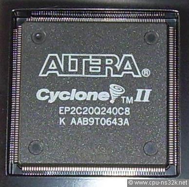
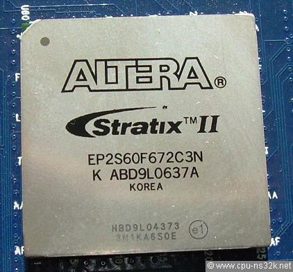
Fig. 1. Two different FPGAs from one vendor.
FPGAs are offered with different characteristics. The left photo above shows a typical low-cost FPGA device. Its package is made of plastic. The right photo above shows a high-end FPGA device in a metal case. The high-end device offers more capacity in terms of configuration bits and higher speed (typically double the speed of low-cost devices). The result is that the device consumes more power and therefore requires a more expensive package.
The different components of a FPGA are described in the following sections.
1. Logic Elements
The logic element (LE at Altera) or logic cell (LC at Xilinx) is the fundamental building block of any FPGA. Figure 2 shows the principal function.
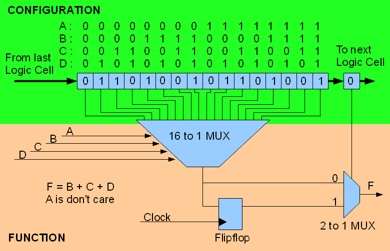
Fig. 2. The basic FPGA logic element.
The genuine idea for the realization of FPGAs was the way to get a logic element programmable by the customer. For this purpose the logic element is composed of two parts : a configuration memory and a functional part. The configuration memory is organized as a shift register. The output of one shift register is connected to the input of the next shift register. With thousands of logic elements in a FPGA the shift register gets very long. But if it is clocked at 1 MHz or even more the loading is done in less than one second.
All outputs of the shift register cells are connected inside the logic element to the functional part. In the example in figure 2 the rightmost shift register cell selects a combinatorical or a registered output (flipflop path). The remaining 16 outputs feed a 16 to 1 multiplexer. Every combination of the four inputs A, B, C and D selects a different shift register cell. Therefore any function with four variables can be defined. In the example the sum of three variables is calculated which is also the xor function of the three variables. This is the sum part of a full adder. The carry part of the full adder is calculated in another logic element which is connected to the same inputs B,C and D.
In the example the input A is "don't care". This means that the output F does not depend on the value of the input A. This is achieved by simply duplicating the content of the shift register for A="0" to A="1".
Up to 16 logic elements are grouped together. They share the same inputs and control signals. For example the clock of the flipflop is a control signal which is used very often. The reset signal is another control signal. The FPGA vendors makes the functional part very fast. This means big transistors and a lot of current. On the other side is the configuration part which must be small and can get slow. In 2013 even the smallest FPGAs has 20000 LEs and the biggest ones have hundreds of thousands of LEs.
2. Memory Blocks
Memory blocks in a FPGA are small SRAMs. They are very useful to build buffers, FIFOs, or ROMs. The size of a memory block is fixed. It maybe any value between 2048 bits and 524288 bits depending on what the vendor thinks is the best compromise. For the customer one memory block of a given size can be configured to different values, for example 128 * 32 bits, 512 * 14 bits, 1024 * 3 bits, 2048 * 2 bits ... If an application needs more bits than one memory block provides the design software uses automatically multiple memory blocks.
Memory blocks need always a clock. A nice feature is the definition of their content at power-up. This can be used for a ROM in an embedded application. A standard application for memory blocks is a FIFO. A FIFO is a "first-in,first-out" memory with two ports : one port is used for writing and the other port is used for reading (Stack is a LIFO memory : "last-in,first-out"). The control logic is build with logic elements and guarantees that the first word written is the first word read. Small FPGAs have less than hundred memory blocks. Large FPGAs provide more than thousand memory blocks.
3. PLLs
A Phase-Looked-Loop or PLL is one of the most important building block in modern electronic systems. The circuit is used to generate a clock signal based on a reference clock signal. Depending on the configuration the generated clock may be higher or lower than the reference clock. Many applications need a high frequency clock signal which can not be generated cost-effectivly by an oscillator. And most applications need more than one clock signal. Therefore today even cheap FPGAs have four PLLs.
4. Multipliers
Multipliers were added late in time to the fixed functions in a FPGA. This became necessary after FPGAs were used in DSP applications. For sure multipliers can be build with logic elements. But they consume a lot of ressources. Fixed functions need much less silicon area. In addition they are much faster. Today multipliers provide up to 27 bits in wordlength and can be cascaded for greater length. They are available in the same amount like memory blocks.
5. I/O Pins
I/O pins are configurable too. For example an I/O pin can act as an input, as an output or as a bidirectional pin. There are newer I/O standards which require a pair of pins, for example LVDS (low voltage differential signaling). The usage of the true signal and the complement signal allows higher signaling speeds. Input pins have a configurable pull-up. The current drive capability of output pins is configurable too. This is important because many outputs switching at the same time generate noise in the chip. Current values should be always as low as possible. One of my first FPGA design with a DRAM did not work stable until I lowered the output current values for the pins driving the DRAM.
6. Transceivers
A special form of I/O is the transceiver. The I/O standard used is some kind of LVDS. For performance reasons they use dedicated pins for input and ouput. But the result is an impressive multi-gigabit data rate. For example SATA needs transceivers to transfer 3 Gbits/s. DVI is another application. Cheap FPGAs don't have transceivers.
A transceiver block in a FPGA contains mainly the logic for converting high speed serial data into low speed parallel data and vice versa. This conversion is necessary because the FPGA can not work directly at the frequency of the high speed serial signals.
7. Interconnects
In a standard chip the interconnect between all circuit elements consists of simple wires. In a programmable device the connection between elements is unknown until the customer is defining the function of the chip. Therefore the "function" of a wire is replaced by a "configurable interconnet" in a FPGA. The datasheets of the FPGA vendors describe only the high-level view of the interconnect structure. Figure 2 shows an example of how a configurable interconnection may be build.
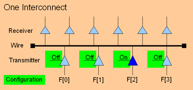
Fig. 2. A configurable interconnect circuitry.
The wire of a configurable interconnect is connected to multiple transmitters and receivers. Each transmitter has a configuration bit which enables or disables the transmitter. Enable means the transmitter is driving the wire. Disable means the transmitter is in a high impedance mode and therefore not driving the wire. Only one transmitter can be enabled at any time. The receivers can be always on. It may be useful to configure them in an "off" mode to save power if they are not used.
Interconnect delay plays an important role in the total propagation delay in FPGAs. But faster interconnect requires more power. Todays huge FPGAs burn already a lot of power in the interconnect. This is the main reason why ASICs and standard chips like mircoprocessors are more power-effective or simply faster than FPGAs.
In a FPGA the interconnects are arranged in rows and columns. For example Altera's FPGAs have many kinds of interconnects. Figure 3 gives an overview.
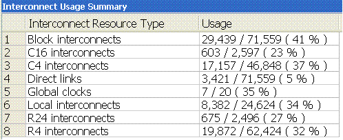
Fig. 3. The interconnect statistic of a FPGA design.
The interconnect statistic is reported by the design compiler. C16 and C4 are column interconnects. R24 and R4 are row interconnects. The numbers 4,16 and 24 tells you how long an interconnect is. There are many more short interconnects than long ones. Block interconnect, direct links and local interconnects are placed only between adjacent logic elements. The global clocks are used for clock signals and other very important control signals like reset.
Most of the configuration bits of a modern FPGA are used for the interconnect. The function of a design is easy to compile and easy to map to the given elements. But it can be very difficult to find a solution for the required routing. If your design is using more than 80% of the available resources and the constrains are tight the time used for the compile process is long enough for a coffee break ...
Next chapter: Architecture